



Global Trade News
Global Trade News
SCHEDULE YOUR INTERVIEW 
  • Home
  • Categories
    • Policy Pulse
    • Compliance Corner
    • Market Movers
    • Trade Trends
    • Export Essentials
    • Import Insights
    • Regulatory Roundup
    • Global Trade News Blog
    • More Spotlights
    • More Videos
October 12.2026
7 Minutes Read

Industry Experts Discuss the Impact of Unified Control on Manufacturing Productivity

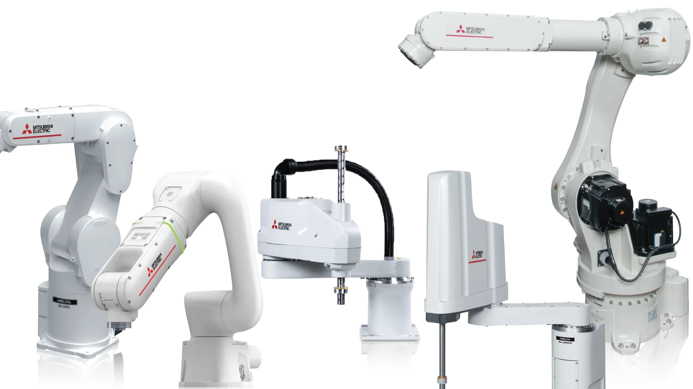
Imagine a manufacturing floor where CNC machines, robots, and control systems seamlessly communicate and coordinate as one unified entity. This integrated approach, led by unified control manufacturing experts at Mitsubishi Electric US, Industrial Automation, not only optimizes productivity but also empowers manufacturers with real-time insights and operational agility. In this article, gain exclusive insights into how unified CNC and robot controls solve complex manufacturing challenges, boost efficiency, and prepare factories for the future of AI-driven automation.

Understanding Unified Control in Manufacturing: An Overview

What Is Unified Control and Why It Matters in Modern Manufacturing

Unified control manufacturing experts define unified control as the integration of CNC controllers, robot controllers, and master PLCs into a single, coordinated system that manages the entire manufacturing process holistically. According to Scott Strache, Sr. Product Manager (Mechatronics), and Dan Zachacki, Sr. Product Manager (Controller, Motion, and Visualization)"Having a system where all these different sections of the machine itself can coordinate together and speak to one another gives you much better visibility to diagnose larger issues instead of looking at individual components.

On the factory floor, this means that components such as CNC machines cutting parts and robots moving those parts from station to station operate in harmony under one control umbrella. Rather than troubleshooting machines one by one when problems arise, operators get a comprehensive view of the entire production line's health and performance. This unified communication is essential for identifying bottlenecks and quality issues early, enabling swift corrective action that can boost throughput and reduce downtime significantly.

Challenges of Separate Systems and the Benefits of Integration

Historically, manufacturing lines run different components with isolated control systems—each with their own protocols and data streams. This segregation creates inefficiencies, as pinpointing the root cause of production slowdowns requires sifting through siloed machine data. It also complicates maintenance, requiring specialized knowledge for each system and increasing response times when machines break down.

By contrast, unified control systems break down these silos through integration, enabling a synchronized factory environment. This coordination helps manufacturers respond faster to production changes and quality control demands. The result is a smarter, more agile manufacturing process that supports just-in-time delivery and higher product quality.

For manufacturers seeking practical strategies to implement these concepts, exploring the latest insights on trade regulations and market trends can provide valuable context for aligning automation upgrades with evolving industry standards and global supply chain demands.

Modern industrial assembly line showcasing unified control manufacturing experts monitoring interconnected CNC and robot controls

How Intelligent Controls and Control Fabric Enhance Manufacturing Efficiency

The Role of Intelligent Controls in Reducing Downtime and Increasing Throughput

Intelligent controls are at the core of this efficiency revolution. Scott Strache emphasizes, "By tying in CNC, robot, and overall production line manufacturing with PLCs and SCADA, you can run lights out 24/7 automatically, resulting in less downtime and more ROI on your equipment." This extended runtime capability means factories can operate continuously without human intervention—maximizing production output and capital utilization.

Beyond just increasing uptime, intelligent controls generate predictive maintenance alerts by analyzing equipment data in real time. This foresight helps maintenance teams intervene before a machine fails, transforming maintenance from reactive firefighting to proactive care. Together, these improvements drive a significant boost in manufacturing throughput and reduce costly unplanned stoppages.

Control Fabric: Seamless Communication Across Devices and Networks

Another transformative concept is control fabric technology that acts as the communication backbone interlinking diverse devices and control systems within a plant. Where once proprietary networks limited device compatibility, modern control fabric supports multiple protocols such as EtherCAT, EtherNet/IP, ProfiNet, CIP Safety, PROFINET and PROFIsafe, ensuring seamless data flow across equipment of varying age and brands.

This expansive compatibility allows manufacturers to unify their control architecture gradually without needing to overhaul existing systems. It empowers devices to “speak the same language” in a factory ecosystem, supporting complex automation scenarios and future scalability.
Futuristic manufacturing factory floor with robotic arms and CNC machines operating in harmony over a control fabric network

Building Automation and Gradual Integration: Practical Steps for Manufacturers

Integrating Unified Control into Existing Plants Without Full Replacement

For many manufacturers, the idea of replacing all existing equipment to adopt unified control can feel overwhelming and costly. Scott Strache shares that Mitsubishi Electric’s approach centers on compatibility and gradual upgrades: “If you’re running everything with one vendor, such as Mitsubishi, compatibility from older equipment to newer equipment means you don’t lose much time integrating upgrades. You can implement unified control incrementally while continuing production.”

This phased approach allows manufacturers to start by upgrading a single machine or station, validating benefits such as improved throughput or reduced downtime. Over time, additional upgrades can build out a unified ecosystem, reducing risks and capital expenditure spikes.

Experienced industrial technician upgrading legacy manufacturing equipment with unified control interfaces

Starting Small: Use Cases to Demonstrate Value and Expand Automation

Dan Zachacki advises manufacturers to identify key use cases before automating broadly: “Pick a specific objective like improving product quality or increasing machine uptime, then automate that area first. Once value is demonstrated, you can scale unified control throughout the plant.” This focused strategy helps secure early wins and stakeholder buy-in.

By following a curated path aligned with specific manufacturing goals, plants can evolve their automation footprint logically instead of making sweeping, disruptive changes. This agility is crucial when balancing ongoing production demands with technology modernization.

Impact on Operators and Maintenance: Evolving Roles with Unified Control

Manufacturing operators reviewing predictive maintenance alerts on digital tablet under unified control systems

From Reactive to Proactive: Predictive Maintenance and Operator Efficiency

Unified control not only reshapes machinery coordination, but it also transforms workforce roles. Operators can oversee multiple lines simultaneously, focusing on monitoring integrated dashboards instead of manual machine tending. Maintenance teams can leverage predictive data to schedule interventions before breakdowns occur, reducing downtime risks and unplanned repairs.

Scott Strache, explains, “The workplace today doesn’t have the labor to run multiple lines manually. Robots combined with intelligent controls and unified data enable a single operator to manage multiple projects. Maintenance becomes more proactive, using predictive tools rather than reacting to failures.”

Simplifying Programming: One Platform for CNC and Robot Control

One key efficiency improvement is simplifying the programming ecosystem. Dan Zachacki highlights the advantage of Direct Robot Control (DRC), which allows operators to program both the CNC and robot using the same familiar G-code programming language: “This means you don’t need separate programmers for robots and CNCs. One skilled technician can program and maintain both pieces of equipment, improving workforce flexibility and reducing training complexity.”

Future Trends: AI, Real-Time Data, and the Evolution of Unified Control

Preparing for AI-Driven Manufacturing and Workforce Changes

Looking to the horizon, unified control manufacturing experts see AI becoming a key enabler of even smarter factories. Dan Zachacki notes, "Unified control will become much easier to implement as AI agents perform tasks like maintenance management and communicate across diverse networks and devices. "

AI promises to revolutionize maintenance with autonomous diagnostics, optimize cycle times in real time, and support fully lights-out manufacturing operations. As the workforce evolves with retiring experienced technicians and new hires trained in AI and predictive analytics, manufacturers must start laying the foundation now.

The End of Proprietary Networks: Embracing Connectivity and Compatibility

Gone are the days of closed, proprietary control networks. Today’s manufacturers demand multi-protocol compatibility to future-proof their automation assets. Scott summarizes this shift: “Devices have connectivity built-in, supporting EtherCAT, PROFINET, and more. Customers want their equipment to talk to each other no matter the make or model. This open connectivity is the future of unified control. ”

High-tech manufacturing control room with AI managing robotic and CNC systems through unified control

Common Questions About Unified Control Manufacturing Experts

  • What are the main benefits of unified control in manufacturing?

  • How can manufacturers integrate unified control with legacy equipment?

  • What role does AI play in the future of unified control?

  • How does unified control affect operator and maintenance roles?

Answers to Frequently Asked Questions

Question

Answer Summary

Benefits of Unified Control

Improved coordination, reduced downtime, increased throughput, and better data insights.

Integration with Legacy Equipment

Gradual implementation with compatible vendor equipment to avoid full replacement.

AI's Role

Enables predictive maintenance, real-time optimization, and autonomous decision-making.

Impact on Roles

Shifts operators and maintenance from reactive tasks to proactive management and multi-skilled roles.

Key Takeaways from Industry Experts on Unified Control Manufacturing

  1. Unified control enables holistic visibility and coordination across manufacturing systems.

  2. Intelligent controls and control fabric reduce downtime and improve ROI.

  3. Gradual integration allows manufacturers to modernize without disrupting production.

  4. Operator and maintenance roles evolve towards predictive and multi-disciplinary functions.

  5. AI and connectivity will drive the next generation of unified control solutions.

Conclusion: Embracing Unified Control for Competitive Manufacturing

Scott Strache emphasizes, "If you haven't started automating your manufacturing floor, you're already behind the times. The future belongs to those who embrace unified control and AI-driven solutions today."

As you consider the next steps for your manufacturing operations, staying informed about the broader landscape of trade regulations and market shifts is essential for making strategic automation decisions. The world of unified control is rapidly evolving, and aligning your technology roadmap with global trends can unlock new opportunities for growth and resilience. For a deeper dive into the latest developments shaping the industry, explore the comprehensive coverage and expert perspectives available at Global Trade News. Discover how forward-thinking manufacturers are leveraging unified control and automation to stay ahead in a competitive global market.

Have industry insights or news tips? Reach out and join our network of global trade professionals today! Schedule your interview with Global Trade News.

Sources:

  • Mitsubishi Electric US, Industrial Automation


  • Global Trade News

3 Views

Write A Comment

*
*
Please complete the captcha to submit your comment.
Related Posts All Posts
10.12.2026

Advanced Packaging: Why Inspection Matters

Picture a state-of-the-art semiconductor manufacturing line: technicians in cleanrooms intently watching silicon wafers and digital dashboards, each inspection and micro-adjustment determining if millions in product value will be realized or lost. In this high-stakes, zero-defect world, advanced semiconductor packaging inspection isn't just another step—it's the gatekeeper to both yield and business success. This article breaks down what every plant manager, process engineer, and manufacturing leader needs to know to stay ahead in the competitive landscape of advanced packaging.Setting the Scene: Why Advanced Semiconductor Packaging Inspection Is a Make-or-Break InvestmentFor manufacturers in the semiconductor industry, adopting advanced semiconductor packaging inspection is no longer optional—it's essential for meeting yield, quality, and throughput goals. Modern packaging formats, such as panel level and wafer level packaging, rely on combining dozens or even hundreds of chips with precise placement, alignment, and connections. Each additional layer of complexity—from flip chip assemblies to die attach steps—makes the inspection system's job even more critical. Defects that once went unnoticed now threaten entire batches and, ultimately, the bottom line. Investing in a high-performance inspection system is not just risk mitigation: it’s a trigger for measurable process improvement, cost savings, and customer trust. Yet, with tight margins and rapid innovation cycles, today's decision-makers must balance technical due diligence with real-world operational insights.Real-World Challenges in Modern Packaging LinesAchieving quality control in today’s advanced packaging lines is no small feat. Defects like alignment errors, delamination, die placement faults, shorts, and opens can emerge during wafer level or panel level processing. Inspection systems face the herculean task of detecting these minute faults in real time, avoiding both false calls and missed detections that could stall production or push bad units downstream. The integration of multiple process steps—like solder paste printing, flux deposit, and applying redistribution layers—demands a comprehensive approach. Each operation can introduce new variables, making measurement data from inspection systems an invaluable feedback loop for process improvement and cost control.For manufacturers seeking to optimize their inspection strategies, understanding the latest trends in global trade and technology adoption can provide a competitive edge. Industry news and regulatory updates often influence equipment choices and process standards, as highlighted in recent coverage on Global Trade News, which explores how evolving market dynamics are shaping semiconductor manufacturing worldwide.Observations From Industry Leaders on Advanced Packaging and InspectionIndustry veterans emphasize that the shift to advanced packaging isn’t just technological; it’s strategic. Companies like TSMC, Samsung, and Amkor Technology have set new benchmarks for inspection standards, and their leadership inspires supply chain partners to follow suit. According to operations leads, robust inspection not only ensures product quality, but also underpins company reputation and customer relationships. The consensus: cutting corners on semiconductor inspection is a risk few can afford in a market where defect rates directly impact profitability and delivery schedules.What You’ll Learn About Advanced Semiconductor Packaging InspectionCore principles of advanced semiconductor packaging inspectionState-of-the-art inspection systems and their practical functionsKey problems solved by inspection technology in packagingFactors to weigh before adopting new inspection systemsCurrent industry trends, examples, and expert observationsUnderstanding Advanced Packaging for Semiconductors: Basics and Market DriversDefining Advanced Packaging and Its Growing RelevanceAdvanced packaging refers to innovative techniques that stack, layer, or interconnect multiple semiconductor components—sometimes using entirely new panel level, wafer level, or die level methods—to create more compact, powerful, and versatile electronic devices. As devices shrink, performance demands soar, and the need for low-latency electrical connections increases. The rise of these packaging techniques is spurred by trends such as 5G, IoT, AI, and cloud computing, which all require greater integration and reliability. Advanced packaging formats, including 3D integration, flip chip assembly, and clad laminate designs, enable higher performance at reduced form factors, but they also raise the stakes for both process and inspection precision.Panel Level, Wafer Level, and 3D Integration: Technology BreakdownsThe three dominant methods in advanced packaging are panel level packaging (PLP), wafer level packaging (WLP), and 3D integration. In PLP, entire panels (larger than traditional wafers) are processed, increasing throughput but amplifying the risk if a defect propagates. WLP processes chips while still mounted on their original wafer, shrinking device footprints and boosting performance. 3D integration stacks dies vertically with micro-bumping, creating a true connectivity platform with significantly denser interconnects. While these approaches enable remarkable performance gains, they each introduce unique inspection challenges due to more intricate die attach, patterning, and electrical connection steps.What is Advanced Packaging for Semiconductors?Answer:Simply put, advanced packaging for semiconductors is the use of innovative, multi-layer assembly formats like panel level, wafer level, and 3D integration to optimize the performance, density, and size of semiconductor devices. By leveraging finer control over die placement, redistribution layer formation, and multi-chip stacking, manufacturers enable higher device performance in smaller footprints. However, the increased complexity of these methods drives the need for even more sophisticated semiconductor inspection solutions throughout the process.Inspection Needs Created by Miniaturization and ComplexityThe miniaturization trend in semiconductor packaging pushes both size and precision limits, magnifying the consequences of undetected defects. As die level parts decrease to sub-millimeter scale and wafer level interconnects pack even closer, routine visual inspections become nearly impossible. Problems like foreign material inclusions, patterning errors, and flux deposit inconsistencies demand technological solutions well beyond manual or legacy equipment. Thus, advanced inspection systems—combining optical, X-ray, and even AI analysis—have become the backbone of modern quality control in packaging lines.What is Semiconductor Inspection?Answer:Semiconductor inspection encompasses automated and manual processes designed to detect, classify, and trace defects throughout the chip manufacturing and packaging lifecycle. Its purpose is to verify that each die, wafer, or packaged device meets tight technical and reliability standards. Advanced inspection systems conduct non-destructive tests using a variety of optical, electrical, and metrology tools. For advanced packaging, inspection takes place at multiple steps—from initial die placement to level integration—helping manufacturers reduce false call rates, catch process drift, and ensure robust electrical connections.Core Capabilities of Advanced Semiconductor Packaging Inspection SystemsThe heart of a modern inspection system is its ability to not only spot visible and sub-visible defects but also supply actionable data for process feedback. Capabilities include high-resolution imaging, real-time defect classification, advanced pattern recognition, and seamless data logging for traceability and regulatory compliance. Today’s inspection systems integrate IoT-enabled sensors and AI to enhance predictive maintenance and process optimization. For plant managers and operations teams, this means faster root-cause analysis, lower scrap rates, and higher value per processed wafer or panel.Why Inspection Systems Are Critical to Advanced Packaging SuccessKey Defects Detected by Semiconductor Inspection SystemsShorts and opensDelaminationAlignment errorsForeign material inclusionsPatterning defectsRole of Inspection in Yield Improvement and Cost ControlSuperior inspection systems aren’t solely about defect detection—they enable yield improvement and provide cost leverage. By identifying faults early (such as delamination or flux deposit issues), inspection prevents defective units from contaminating final output, reducing rework and scrappage. For high-throughput die level and panel level lines, a single missed alignment error may impact thousands of units. Comprehensive measurement data supports process engineers in making evidence-based changes to the manufacturing process, ultimately reducing operational expenses and boosting first-pass yield rates."By pinpointing problematic steps with precision inspection, we’ve seen direct yield improvements of several percentage points, with ripple effects through our supply chain and customer satisfaction scores." — Senior Process Engineer, Leading FoundryIndustry-Leading Solutions: Advanced Semiconductor Inspection System ComparisonSystemDetection AccuracyThroughputUse CasesIntegration EaseInspection Technology TypeSystem ASub-micronHighPanel level, wafer levelPlug-and-playOptical + AISystem B~1 micronModerateDie level packaging, flip chipCustom integrationX-ray, visualSystem CSub-micronVery HighHigh-volume wafer levelModularHybrid (Optical/X-ray)Overview of Competing Approaches in Inspection SystemsThe market offers a variety of semiconductor inspection systems, each catering to different packaging formats and production needs. Some prioritize ultra-high-resolution defect detection for die level and panel level processing, while others focus on speed and minimal operator intervention. New systems increasingly leverage AI for real-time pattern recognition and process drift alerts. When evaluating solutions, consider factors like integration with facility MES, data traceability, and support for non-destructive testing, as these can markedly affect both yields and total cost of ownership.Which Companies Are Known for Their Advanced Semiconductor Packaging?Answer:Major industry players advancing panel level and wafer level packaging include:Market Leaders in Panel Level and Wafer Level PackagingTSMCASE GroupAmkor TechnologyIntelSamsungThese leaders set benchmarks in integrating inspection systems into high-complexity packaging lines, often driving the adoption of next-generation process control techniques and raising the bar for semiconductor inspection globally.Does TSMC Do Advanced Packaging?Answer:Yes, TSMC (Taiwan Semiconductor Manufacturing Company) is renowned for its advanced packaging services. It offers leading-edge panel level and wafer level solutions that include technologies like CoWoS (Chip-on-Wafer-on-Substrate) and InFO (Integrated Fan-Out). TSMC’s efforts have solidified its status as a global technology leader in the semiconductor industry.TSMC's Role in Driving Inspection Standards and TechnologyTSMC’s internal standards for inspection are among the strictest in the world, especially regarding panel level and wafer level packaging. By collaborating with toolmakers, TSMC helps develop new semiconductor inspection systems that are quickly adopted industry-wide. This continuous innovation ensures that even as advanced packaging complexity increases, defect rates are kept exceptionally low, with lessons filtered out to the rest of the ecosystem.What to Consider Before Investing in Advanced Semiconductor Packaging Inspection SolutionsKey Questions for Manufacturers and Operations LeadersIs your existing equipment compatible with next-generation inspection systems?What are your data handling and traceability requirements?Will facility modifications be necessary to support new systems?How do you evaluate the cost of ownership against expected value?What change management and operator training needs do you face?Potential Mistakes, Limitations, and Implementation PitfallsCommon pitfalls include underestimating facility space requirements, neglecting to address data integration with MES/ERP, and insufficient training for operators, all of which can undermine the benefits of an advanced semiconductor packaging inspection system. Decision-makers should be wary of false call rates from poorly tuned inspection algorithms, as well as the risk of selecting systems that cannot scale with future process changes or packaging technique innovations. Avoid shortcuts: a short-term cost saving can result in long-term quality or throughput losses.Lists of Practical Specifications and Buying GuidelinesChecklist: Evaluating a Semiconductor Inspection System for Your FacilityCompatible with your existing process and packaging formats?Detection accuracy meets your product standards?Integration support with factory MES and traceability systems?Throughput matches projected production volumes?Vendor support for installation, calibration, and ongoing training?Questions to Ask Vendors About Advanced Packaging InspectionHow is the system calibrated for different wafer and panel sizes?Can it detect key defect types (delamination, shorts, opens, patterning errors)?What ongoing maintenance, software updates, and training does the company offer?How does the system support AI/automation features and future expansion?Key Takeaways: Advanced Semiconductor Packaging Inspection for BuyersAdvanced semiconductor packaging inspection drives both quality and business valueSuccessful implementation requires technical due diligence and real-world case assessmentIndustry leaders set benchmarks for process and technologyFrequently Asked Questions About Advanced Semiconductor Packaging InspectionWhy are inspection systems essential in semiconductor assembly?Inspection systems are crucial because they ensure every packaged device meets strict quality and reliability requirements, catching defects early in the manufacturing process to reduce scrap, rework, and field failures. By enabling real-time detection, they support overall yield improvement and facilitate data-driven process optimization for advanced, complex packaging lines.Can legacy inspection tools keep up with advanced packaging?Legacy tools often fall short in detecting minute or sub-surface defects seen in modern wafer level, panel level, and 3D-packaged devices. As die sizes shrink and complexity grows, only next-generation semiconductor inspection systems offer the needed resolution, integration, and data capabilities to support process control and minimize false call rates.What is the ROI timeframe for new inspection systems?While ROI depends on your facility’s output and baseline defect rates, many users observe measurable improvements in yield and defect reduction within the first several months post-installation. The most significant gains come from reducing scraps, rework, and liability costs by catching defects as close to their source as possible.Industry Voices: What Manufacturers Are Saying About Advanced Packaging and Inspection"After deploying an advanced inspection system in our level packaging line, we saw a marked decrease in false calls and a faster feedback loop for process adjustments. The upfront effort in vendor selection and operator training paid for itself through improved quality control and customer satisfaction." — Operations Manager, Major Semiconductor ManufacturerSee Advanced Semiconductor Packaging Inspection in ActionPlant Tour of a Modern Semiconductor Packaging Line Using Advanced InspectionInterview With an Application Engineer on Inspection Challenges and Success StoriesLooking Forward: The Evolution of Advanced Semiconductor Packaging InspectionAnticipated Developments in AI and Automation for Inspection SystemsThe future of semiconductor inspection points toward smarter, more autonomous systems powered by AI and machine learning. Real-time analytics, predictive maintenance, and adaptive algorithms promise ever-higher throughput and defect detection rates for both wafer level and panel level lines. Enhanced robotic automation could allow for seamless line reconfiguration and new packaging format support, ensuring that inspection technologies keep pace with growing device complexity and shrinking form factors.How Buyer Expectations and Market Demands Are Shaping Future SolutionsBuyer expectations are shifting toward “plug-and-play” systems with rapid ROI, easy data integration, and robust traceability. Market competition is pushing suppliers to offer not only traditional inspection system capabilities but also cloud-enabled analytics, automatic defect classification, and scalable integration for future process nodes. Manufacturers evaluating new systems should consider not only technical features but also the degree of vendor support, system flexibility, and upgradeability to secure long-term value and adaptability in a fast-evolving market.Ready to Navigate the Future of Advanced Semiconductor Packaging Inspection?Have industry insights or news tips? Reach out and join our network of global trade professionals today! Schedule your interview with Global Trade News.As the semiconductor landscape continues to evolve, staying informed about global trade developments and regulatory shifts is essential for forward-thinking manufacturers and supply chain leaders. For a broader perspective on how international markets, policy changes, and technology trends are influencing the future of advanced packaging and inspection, explore the latest insights and expert analysis at Global Trade News. Whether you’re seeking to anticipate market disruptions or identify new growth opportunities, leveraging up-to-date intelligence can help you make smarter, more resilient business decisions in this dynamic industry.

10.10.2026

Advanced Semiconductor Packaging: Production Challenges

Imagine walking through a state-of-the-art semiconductor facility: engineers move seamlessly between consoles, robotic arms position microscopic components, and real-time data pulses across glowing displays. This futuristic scene underscores a critical point—advanced semiconductor packaging is at the heart of today's innovation in electrical components, shaping everything from consumer devices to mission-critical industrial systems. In this guide, learn what drives the industry forward, the hurdles encountered in production, and actionable strategies to help your business stay ahead in a fast-evolving market.Introduction to Advanced Semiconductor PackagingAdvanced semiconductor packaging refers to the cutting-edge techniques and materials used to connect, protect, and enable the next generation of electrical components. Unlike traditional packaging, these advanced methods support higher device performance, more compact form factors, and improved energy efficiency. As technology pushes boundaries, robust packaging solutions have become more essential—not only do they affect device speed and functionality, but they also impact system reliability and total cost of ownership. Whether you’re driving innovation as a manufacturer, optimizing plant operations, or making decisions on new equipment investments, understanding these trends can lead to smarter purchasing, better implementation, and new business opportunities.As the demand for powerful, miniaturized electronics grows, advanced packaging designs like 3D system-in-package (SiP), wafer-level packaging (WLP), and fan-out solutions are fast becoming the norm. This transition brings both technical challenges and strategic opportunities for companies seeking to expand their offerings, increase yield, and serve high-reliability sectors like automotive, industrial automation, and telecommunications. What you'll learn in this guide to advanced semiconductor packaging:The core production challenges in advanced semiconductor packagingLatest industry strategies for overcoming manufacturing hurdlesBusiness opportunities and implementation tipsReal-world examples from leading electrical components manufacturersExpert commentary and actionable adviceThe Evolving Landscape of Advanced Semiconductor PackagingThe landscape for advanced semiconductor packaging has shifted rapidly in recent years, driven by the relentless demand for higher-performing, smaller, and more reliable electrical components. Major industries including automotive, wireless communications, IoT, and computing are now relying on leading-edge packaging strategies to achieve breakthroughs in system speed, power efficiency, and device integration. This evolution does not merely follow trends—it fundamentally redefines the capabilities and economics of producing cutting-edge electronics. Adoption is no longer limited to the biggest industry players; even mid-size manufacturers now seek advanced packaging to deliver a competitive edge and unlock new markets.Companies must also weigh the operational and strategic priorities that come with this shift. As packaging methods become more complex, manufacturers are challenged to invest in new equipment, update technical skill sets, and adapt processes for quality assurance. Successful leaders approach this evolution with careful planning—identifying the right packaging architecture, finding suppliers with proven experience, and building flexibility into their manufacturing roadmap to keep up with dynamic industry needs.For manufacturers looking to navigate these complexities, staying informed about the latest trade regulations and market shifts is essential. Accessing up-to-date industry insights, such as those provided by Global Trade News, can help companies anticipate supply chain disruptions and align their packaging strategies with global trends.Observations on demand and usage across electrical components sectorsDemand for advanced semiconductor packaging is especially prominent in sectors requiring high reliability and performance. For instance, automotive manufacturers need packaging that withstands extreme environments and long operational lifespans. In the telecommunications industry, speed and bandwidth requirements drive adoption of complex multi-chip module designs. Even consumer electronics—smartphones, wearables, and tablets—now mandate the use of 3D-packaged chips to fit more power into smaller, slimmer form factors. Large electrical component makers are leveraging these advances to introduce smarter, multifunctional systems, while mid-tier firms look to advanced packaging to differentiate their offerings.As observed by market analysts, "Advanced semiconductor packaging is redefining the roadmap for electrical components, delivering performance and reliability that legacy packaging simply can't match. " This transition reflects a broad conviction: leveraging advanced techniques isn’t just a technical upgrade, but a strategic business imperative for staying relevant and competitive as technology cycles accelerate."Advanced semiconductor packaging is redefining the roadmap for electrical components, delivering performance and reliability that legacy packaging simply can't match." — Industry Analyst Key Production Challenges in Advanced Semiconductor PackagingWhile the benefits are substantial, adopting advanced semiconductor packaging comes with its own set of production challenges. Manufacturers often encounter hurdles ranging from new material requirements to the tighter tolerances of miniaturized designs and maintaining consistently high yields at scale. Understanding and proactively addressing these technical and operational obstacles is crucial for companies looking to succeed in this competitive field. The complexity involved calls for collaboration across engineering, supply chain, and plant operations to identify where bottlenecks may arise and how best to resolve them without compromising output quality or profitability.Some of the most significant hurdles manufacturers face include the integration of diverse new materials, challenges related to assembling increasingly miniaturized and high-density components, and sophisticated thermal management demands that—if not properly addressed—can threaten the reliability and effectiveness of even the most promising products.Material integration and compatibility issuesAdvanced semiconductor packaging often calls for a mix of novel materials: high-density organic substrates, advanced underfill compounds, and specialized solder alloys. Each additional material introduces compatibility risks—coefficients of thermal expansion may not match, new chemical interactions could occur, and electrical properties must meet tighter requirements. Addressing these integration issues requires extensive simulation, rigorous validation, and close supplier collaboration. In practice, companies sometimes discover too late that a seemingly minor material mismatch can lead to warping, cracking, or even early device failure. Plant managers and process engineers, therefore, need comprehensive evaluation protocols and a willingness to invest in ongoing materials research.Supply chain reliability also becomes more critical. Shortages or variation in material quality can disrupt the manufacturing flow, leading to increased defects and lengthy troubleshooting. As manufacturers invest in advanced semiconductor packaging, having robust vendor qualification and alternative sourcing plans helps mitigate these material and compatibility risks, ensuring that high-value product runs stay on schedule and meet performance targets.Miniaturization and high-density assembly complexityThe push for smaller, more densely packed chips introduces assembly complexities that are substantially higher than those found in legacy solutions. Finer pitch interconnects, 3D stacking, and through-silicon vias (TSVs) expand the possibility for performance but also escalate the risk of alignment errors, shorts, and process variation. Workers must be retrained on more precise assembly tools, and inspection systems must upgrade to spot sub-micron defects before they propagate through production.Manufacturers often find that their existing equipment can’t handle the demands of advanced assembly processes. New investments in robotics, high-resolution imaging, and automated quality assurance are usually necessary. Plant operations leaders must be prepared to oversee integration of these advanced tools, develop new maintenance protocols, and establish specialized process control measures that prevent quality escapes, thus protecting both yield and reputation.Thermal management and reliability concernsThermal issues represent a persistent challenge in advanced semiconductor packaging. Smaller chips concentrated in high-density packages tend to trap heat more easily than traditional designs, raising the risk of thermal stress, degraded performance, and early failure. Industry leaders now employ advanced heat spreaders, embedded cooling layers, and even micro-fluidic channels within packaging to counteract these risks. The complexity of these thermal management solutions means more testing, specialized materials, and fine-tuned design processes are required from the outset.For manufacturers and engineers, a failure to effectively manage heat can jeopardize entire product portfolios—especially in applications where reliability and duty cycle are mission-critical. The solution includes a mix of advanced simulation (for predicting hot spots), real-time temperature monitoring on the production floor, and collaborating closely with materials science experts to specify and validate the right cooling technologies for each application. Yield optimization and process control strategiesAs advanced packaging pushes the limits of manufacturing miniaturization and integration, yield optimization takes on a new level of importance. Even small inconsistencies—in materials, process steps, or assembly parameters—can quickly escalate defect rates and drive up costs. Leading-edge manufacturers rely on data-driven process control: employing inline inspection systems, real-time analytics, and automated feedback loops to detect and correct drift before it impacts overall device yield.Strategic process improvement is a continuous effort. Engineers should engage in regular root-cause failure analysis, update test protocols as new designs emerge, and collaborate with equipment suppliers for process enhancements. By focusing on both defect prevention and rapid issue resolution, operations teams ensure that the promise of advanced semiconductor packaging translates directly into improved margins and customer satisfaction.Table: Comparing Traditional and Advanced Semiconductor PackagingFeatureTraditional PackagingAdvanced Semiconductor PackagingMaterialsStandard silicon, basic substratesAdvanced materials, high-density interposersForm FactorLarger, simplerMiniaturized, complex 3D structuresThermal SolutionsBasic dissipationIntegrated, high-efficiency coolingCost StructureLower upfront, higher per unitHigher upfront, lower per unit at scaleBusiness Impact: How Advanced Semiconductor Packaging Shapes Electrical Components MarketsAdopting advanced semiconductor packaging impacts every corner of the electrical components industry—from R&D investments to finished product reliability. Companies that get it right can outpace the competition by bringing smaller, faster, and more integrated products to market. On the business front, these gains translate to higher customer value, the ability to enter new verticals, and improved long-term profitability due to reduced failure rates and lower total cost of ownership.However, the transition isn’t without its challenges. Aligning new packaging capabilities with customer requirements, ensuring smooth plant integration, and complying with evolving industry standards requires strategic planning and executive buy-in. Successful implementation starts with a clear understanding of business goals, followed by investments in the right technology, and ongoing support for workforce upskilling and process refinement. Case studies: Implementation in various industriesConsider the automotive industry, where companies have moved to advanced semiconductor packaging to deliver more powerful control units and sensors in autonomous vehicles. These innovations provide real-time responsiveness, reduced failure risk, and longer service life. In industrial automation, advanced packaging methods allow for the integration of discrete and analog devices into robust modules that operate continuously in harsh environments. Consumer electronics firms, meanwhile, employ wafer-level and 3D packaging to launch trend-setting products that outperform rivals in speed, battery life, and design sleekness. Each example underscores the flexibility and impact of investing in cutting-edge packaging solutions tailored to industry-specific needs.Working with experienced packaging partners allows manufacturers to shorten product development cycles and quickly adapt to market demands. This collaborative approach not only accelerates innovation but also gives companies the resilience needed to withstand shifts in global supply chains and regulatory requirements.Advantages over legacy solutions for manufacturers and end usersAdvanced semiconductor packaging delivers tangible advantages: smaller device footprints, faster data transmission, improved energy efficiency, and greater reliability under stress. For manufacturers, this means opening new market segments and strengthening competitive positioning. End users benefit from electronics that last longer, perform better, and support more complex applications without requiring bulky hardware or excess cooling solutions.In a rapidly evolving landscape, legacy packaging simply cannot match these benefits—especially as customers across all segments expect smarter, more reliable electrical components. Choosing the right advanced packaging technology ensures that both manufacturers and their clients stay ahead, regardless of industry fluctuations or technology cycles.Operational considerations before investing in advanced semiconductor packagingBefore making the leap, plant managers and operations leaders should conduct a thorough audit of existing capabilities, technical expertise, and equipment. Advanced semiconductor packaging often requires new process controls, specialized staff training, and updated material handling protocols. Understanding the capital and operational expenditures involved will help ensure realistic ROI expectations. It’s also essential to engage with technology providers and peers to understand common pitfalls and to benchmark best practices.Firms that proactively address these considerations are better positioned to adapt during the implementation phase, limit costly downtime, and deliver finished products that uphold their reputation for quality and reliability in the market.Expert Commentary: Leading Companies on Meeting Production Challenges"Our investment in advanced semiconductor packaging has been crucial for staying ahead in complex, high-reliability markets." — CTO, Major Electrical Components FirmTop firms in the electrical components industry have publicly stated that their move toward advanced semiconductor packaging directly correlates with both their ability to serve demanding new markets and their operational resiliency during market disruptions. Many emphasize that the shift is no longer optional—it’s now a necessary competitive differentiator. The leaders encourage peers to focus on ongoing training for technical teams, robust supplier relationships, and investment in predictive process control systems as keys to success.Their advice: treat the transition as a phased journey, learning from small pilot runs and scaling successes gradually for maximum long-term value. Transparent communications between engineering, procurement, and production teams allows for better anticipation of both technical hurdles and commercial opportunities, ensuring the entire organization is prepared for the complexities that advanced semiconductor packaging can bring.Lists of Common Mistakes and Pitfalls When Transitioning to Advanced Semiconductor PackagingInsufficient evaluation of thermal requirementsUnderestimating material and equipment costsNeglecting employee training in new processesFailure to test for long-term reliabilityBy avoiding these common mistakes, manufacturers safeguard investments and maintain high standards through every phase of deployment and scaling in advanced semiconductor packaging.Key Takeaways for Decision Makers on Advanced Semiconductor Packaging Thoroughly assess production capabilities and challenges before transitioningLeverage industry partnerships for knowledge and resource sharingPrioritize reliability and cost-effectiveness in solution selectionAs with any major operational upgrade, the path to successfully adopting advanced semiconductor packaging begins with due diligence and a focus on strategic value drivers.FAQsWhat industries benefit most from advanced semiconductor packaging?Industries that require high reliability, compact devices, and superior performance benefit the most from advanced semiconductor packaging. This includes automotive electronics, telecommunications, aerospace, industrial automation, and consumer devices like smartphones and wearables. These sectors rely on miniaturized, integrated chips that can perform in demanding environments while delivering energy efficiency and robustness.What are the main drivers for adopting advanced semiconductor packaging over traditional methods?The primary drivers are the need for improved performance, reduced size, and greater reliability in electrical components. Advanced semiconductor packaging supports higher data rates, better thermal management, and enables complex, multifunctional system integration. Manufacturers also turn to advanced packaging to differentiate their products, reduce life-cycle costs, and adapt quickly to changing marketplace requirements.This animated explainer video visually illustrates how advanced semiconductor packaging works, highlighting production challenges, industry innovations, and comparing modern facilities with traditional methods.What are the expected future trends in advanced semiconductor packaging for electrical components?Future trends include the widespread adoption of heterogeneous integration, increased use of AI-driven process control, and ongoing miniaturization of high-performance logic and memory modules. Additionally, improved thermal management technologies, sustainable material sourcing, and greater automation throughout the packaging process are expected. These developments will allow companies to unlock new possibilities in smart devices, edge computing, and advanced industrial systems.Summary: The Future of Advanced Semiconductor Packaging in Electrical Components Advanced semiconductor packaging stands at the forefront of innovation in electrical components. Companies that prioritize strategic onboarding, continuous learning, and reliable supplier networks are best positioned to achieve operational excellence and long-term competitive advantage.As the semiconductor industry continues to evolve, staying ahead requires more than just technical expertise—it demands a keen understanding of global trade dynamics and regulatory shifts. For leaders and innovators seeking to future-proof their strategies, exploring comprehensive resources like Global Trade News offers a broader perspective on market trends, supply chain resilience, and emerging opportunities. Delve deeper into the world of international trade and discover how proactive insight can empower your next move in advanced manufacturing. The journey to industry leadership starts with informed decisions—expand your knowledge and stay connected to the pulse of global innovation.Have industry insights or news tips? Reach out and join our network of global trade professionals today! Schedule your interview with Global Trade News.

10.09.2026

How to choose a semiconductor equipment supplier

Imagine walking through a spotless, high-tech semiconductor fab, where every piece of equipment is mission-critical and every purchasing decision can shape your operation’s future. Whether you’re a seasoned plant manager, a procurement officer, or an engineer tasked with equipment sourcing, the stakes are high: choose the right supplier, and your lines run with world-class efficiency; choose wrong, and you risk costly downtime, compliance headaches, or missed market opportunities.This guide strips away the complexity to answer the biggest questions about procurement for semiconductor equipment. You’ll find clear, practical language on what to look for, which business questions to ask, and how to leverage digital procurement strategies to confidently make the right purchasing decisions in a competitive and fast-evolving landscape.Understanding Procurement in the Semiconductor IndustryWhat is Procurement and Why It Matters for Semiconductor Manufacturers?At its core, procurement is much more than just buying goods or equipment—it’s a strategic business function that governs how a company finds, evaluates, and selects suppliers that are critical to its operations. In the semiconductor industry, where investments in equipment and technology are significant and highly specialized, procurement decisions directly influence manufacturing agility, product quality, compliance, and total cost of ownership.For semiconductor manufacturers, the procurement function involves collaboration between procurement officers, engineers, and purchasing managers to ensure each piece of equipment helps achieve the total enterprise’s objectives—ensuring not only technical capability but alignment with broader supply chain, compliance, and business goals. Robust procurement practices provide a competitive edge by minimizing risk, supporting innovation, and keeping the supply chain resilient in a market where demand shifts rapidly and regulation can change overnight.Key Procurement Challenges in Semiconductor Equipment SourcingNavigating semiconductor equipment sourcing is challenging due to factors like rapidly evolving technology, complex specifications, and intense global competition for limited supplier capacity. Purchasing agents must also consider interoperability with existing ERP solutions, integration with digital manufacturing systems, and the ability of suppliers to meet strict compliance and documentation standards.Compounding these challenges is the fact that procurement officers and supply management professionals must regularly evaluate both direct spend and addressable spend to align with corporate goals. Supplier due diligence, lifecycle management, and benchmarking procurement performance become crucial to avoid costly mistakes. Ultimately, finding suppliers that combine technical excellence with reliability and proactive service is the linchpin to operational success in this high-stakes environment. To further strengthen your supplier evaluation process, consider how digital procurement dashboards can provide real-time tracking of supplier compliance and performance. These tools are increasingly vital for procurement teams aiming to streamline supplier selection and mitigate risk—discover more about their practical impact in real-world scenarios by exploring case studies on digital procurement in action.What You'll Learn About Procurement and Equipment Supplier SelectionThe role of procurement in high-tech manufacturing environmentsStrategic considerations when evaluating semiconductor equipment suppliersRisks, common challenges, and how to avoid costly procurement mistakesKey advantages of digital and electronic procurement approaches Procurement Fundamentals for Semiconductor EquipmentDefining Procurement, Purchasing, and SourcingProcurement, purchasing, and sourcing are interrelated but distinct elements of an organization’s supply management framework. Procurement refers to the end-to-end strategic process of identifying business needs, analyzing markets, engaging in supplier search activities, negotiating contracts, and managing supplier relationships. In contrast, purchasing is the transactional act—placing orders and paying suppliers for goods and services after a supplier has been selected.Sourcing sits between these two, focused on supplier discovery, assessment, and contract negotiation. The procurement department or procurement staff are responsible for orchestrating the entire continuum—from needs assessment to supplier relationship management—often leveraging the expertise of purchasing managers and purchasing agents for the direct execution of buying processes.Differences Between Procurement and Purchasing in Equipment AcquisitionWhen acquiring semiconductor equipment, understanding the distinction between procurement and purchasing is vital. Procurement is holistic: it starts with a strategic review of production needs, supplier markets, and compliance obligations. It evaluates suppliers not just on price but on total value, technical support, compliance, and long-term partnership potential—all critical to high-tech manufacturing.Purchasing, by contrast, is operational. Once the procurement function zeroes in on a supplier, the purchasing agent executes buying orders, arranges payment, and tracks delivery logistics. Organizations with strong procurement practices integrate purchasing seamlessly within the broader framework, ensuring that buying decisions align with the company’s overall supply chain and risk management strategy.Procurement Process Flow – From Needs Assessment to Supplier EngagementThe procurement process in semiconductor equipment can be visualized as a sequence of clearly defined steps, beginning with a needs assessment to specify requirements, followed by search activities to identify qualified suppliers. Next comes a market scan—benchmarking capabilities, capacity, and regulatory history. Supplier evaluation goes deeper, examining ERP solution compatibility, compliance records, and support infrastructure.Engagement proceeds with bid solicitation, in-depth evaluation, negotiation, and contract establishment. The process concludes with delivery, implementation, and ongoing supplier relationship management—supporting both immediate operational needs and long-term enterprise goals. Throughout, procurement officers and purchasing managers are obligated to apply rigorous due diligence, documentation, and benchmarking to mitigate risks and optimize spend under management. Key Criteria for Choosing a Semiconductor Equipment SupplierAssessing Supplier Technical Capabilities and Reliability for ProcurementYour supplier’s expertise can set the tone for the entire production cycle, impacting everything from uptime to product quality. In procurement, it’s crucial to evaluate not only the technology offered but also the supplier’s history of delivering, their ongoing support model, and their responsiveness in critical situations. Check references, examine track records in similar plant environments, and consider their service support, total cost of ownership, and flexibility in customizations.Procurement staff should consistently benchmark suppliers for technical capability, adherence to specification, post-sale support, and their ability to collaborate in continuous improvement. Reliable suppliers often distinguish themselves with proactive compliance, clear technical communication, and transparent cost structures, minimizing surprises and streamlining the overall procurement process for both purchasing managers and engineers.Evaluating Integration Compatibility: Procurement Questions for Digital ManufacturingAs digital manufacturing becomes the norm, procurement departments must ensure that new equipment integrates seamlessly with existing ERP solutions and digital infrastructure. Ask suppliers about interoperability standards, compatibility with plant automation, and data exchange protocols. Addressable spend considerations also include licensing, upgrade paths, and technical support availability.Smart procurement means involving IT and process engineers early in the purchasing decision, using technical checklists, demo tests, and pilot projects to verify real-world compatibility. Procurement officers should demand proof of integration at reference sites or through simulation before committing to any significant equipment acquisition, reducing risk and avoiding downstream costs or delays.Safety, Compliance, and Regulatory Factors in ProcurementSemiconductor equipment procurement is tightly bound to compliance—spanning health and safety, environmental, and sector-specific regulations. Your procurement function must verify supplier certifications, compliance documentation, and their ability to meet international standards. Failing to conduct due diligence exposes your operation to legal and operational risks, delays, and costly revalidation.Procurement managers should request clear records on equipment safety testing, regulatory inspections, and compliance management protocols. Compliance is not a box-ticking exercise; it reflects the supplier’s operational maturity and their role in ensuring your manufacturing agility and eligibility for government procurement contracts or export-driven opportunities. Supplier Evaluation Table: Comparing Your Top Procurement OptionsCriteriaSupplier ASupplier BSupplier CTechnical capabilityIntegration & compatibilityIndustry complianceSupport & serviceTotal cost of ownershipElectronic Procurement: Streamlining the Supplier Selection ProcessHow Electronic Procurement Platforms Improve Decision-MakingElectronic procurement platforms are revolutionizing how manufacturers identify, evaluate, and onboard new suppliers. By digitizing the procurement process, these tools deliver transparency, standardized supplier evaluation, and integration with ERP solutions for end-to-end traceability. Procurement officers can benchmark supplier performance, track compliance in real time, and automate documentation—reducing risk and freeing up procurement staff for more strategic roles.Additionally, electronic procurement unlocks actionable insights using analytics to detect trends in direct spend, addressable spend, and supplier responsiveness. Digital dashboards offer instant access to metrics, ensuring purchasing managers and chief procurement officers can make informed purchasing decisions with confidence—minimizing delays and improving supplier relationships across the global supply chain.Digital Procurement Trends in Semiconductor ManufacturingModern semiconductor manufacturing is increasingly shaped by trends such as cloud-based procurement, real-time supplier ratings, and AI-driven sourcing tools. Digital procurement strategies support supply chain resilience by enabling agile responses to market shifts, automating routine purchasing activities, and providing greater visibility over spend under management.Plant managers and procurement staff benefit from these technologies through reduced paperwork, faster supplier qualification, and enhanced compliance tracking. The ability to capture lessons learned and benchmark procurement performance means continuous improvement becomes embedded in the organization’s procurement and supply management culture. As competition for advanced equipment accelerates, digital procurement gives forward-thinking manufacturers the strategic edge. Government Procurement in Semiconductor Equipment: Compliance and OpportunitiesRegulatory Considerations for Government Procurement ContractsNavigating government procurement for semiconductor equipment demands strict adherence to public procurement procedures, contract guidelines, and often, domestic content rules. Procurement officers and purchasing agents working with public sector clients must prepare thorough documentation, demonstrate transparency, and comply with obligations to apply fair competitive processes.Government contracts may impose specific standards for supplier vetting, cybersecurity, and reporting, setting a higher bar for compliance than commercial contracts. Understanding the layers of regulation and collaborating with legal advisors can ensure eligibility for high-value contracts while minimizing the risk of disqualification or sanction—especially in global semiconductor markets.Navigating Export Controls and National Security in ProcurementSemiconductor procurement is shaped by export controls and national security laws—impacting equipment that contains sensitive technology or intellectual property. Procurement staff must clarify with suppliers any export compliance flags, licensing requirements, and end-use restrictions before finalizing purchasing decisions.Managing government procurement also means tracking changes in international regulations that could affect supply chain continuity. Successful manufacturers involve legal and compliance experts early in the procurement process to safeguard both immediate deliveries and long-term business opportunities, ensuring the company’s procurement function is ready to embrace government and defense-related contracts without risk exposure. Common Procurement Mistakes and How To Avoid ThemOverlooking supplier due diligenceNeglecting integration and supportIgnoring lifecycle costsUnderestimating the need for compliance documentationFailing to benchmark procurement performanceMistakes in procurement can derail your technology investments and operational timelines. Skipping due diligence or failing to properly vet supplier reliability is a common error that leads to performance issues or compliance violations. Not engaging IT and engineering teams can mean compatibility problems with existing ERP solutions or manufacturing automation, resulting in costly integration delays.Savvy purchasing managers also remind their procurement staff to look at lifecycle costs, not just upfront prices. Focusing only on initial savings often ignores expenses related to maintenance, calibration, and future upgrades. Keeping detailed records and performance benchmarks helps chief procurement officers and teams continuously improve purchasing activities and avoid repeated mistakes. Lessons from the Field: Procurement Case Studies in Semiconductor Equipment"Choosing the right supplier doesn’t just impact cost and time-to-market—it shapes your ability to compete globally." – Senior Plant Manager, Leading Semiconductor FabReal-world case studies in procurement illustrate valuable lessons for semiconductor manufacturers. For example, a multinational electronics firm found that by involving procurement officers and IT experts early in the equipment acquisition phase, integration issues were nearly eliminated, reducing project timelines by several weeks. Another company improved its supplier evaluation process by implementing a digital procurement dashboard, allowing real-time tracking of supplier compliance and performance—this led to measurable improvements in supply chain resilience and reduced risk of production stoppages.These stories underscore that effective procurement isn’t just about negotiating price. It requires a strategic partnership with suppliers, rigorous documentation, and a continual eye on technology alignment, risk, and lifecycle value. The most successful organizations treat procurement as a dynamic, evolving process—integrating lessons learned to drive ongoing manufacturing and business success. Explore a concise explainer video that demonstrates procurement workflows in modern semiconductor manufacturing. Featuring animated flowcharts, expert interviews, and direct comparisons of traditional and digital procurement processes, this video brings clarity to complex supplier selection strategies for engineers and plant leaders.People Also Ask: Essential Procurement InsightsIs procurement well paid?Procurement compensation can be competitive, especially within high-value manufacturing industries. Factors influencing pay include the level of responsibility, the complexity of the required knowledge, and experience with supplier negotiations. Many organizations provide advancement pathways for procurement professionals, rewarding expertise in supplier management, compliance, and supply chain optimization.What are procurement synonyms?Synonyms for procurement include sourcing, acquisition, purchasing, supply management, and buying. In the semiconductor industry, these terms often reference specific aspects of selecting suppliers or executing contracts. Understanding procurement synonyms helps new purchasing agents align with established terminology in the field.What is procurement vs purchasing?Procurement involves the end-to-end process of identifying operational needs, qualifying and evaluating suppliers, negotiating contracts, and managing long-term supplier relationships. Purchasing, conversely, refers more narrowly to the act of buying goods and services after a supplier has been selected and approved.What are the 7 stages of procurement?Identifying needsSpecification developmentSupplier sourcingSoliciting and evaluating bidsNegotiation and contractingDelivery and implementationSupplier relationship managementEach of these stages ensures the procurement process is thorough and aligned with both business and operational objectives, supporting a robust supply chain.FAQs for Procurement in Semiconductor Equipment SourcingWhat documents are needed for semiconductor equipment procurement?Typical documentation includes technical specs, compliance certifications, safety records, supplier references, contracts, and implementation checklists.How can teams benchmark procurement success?Procurement success can be benchmarked by tracking supplier performance, cost savings, cycle times, compliance rates, and integration success rates using digital dashboards and regular audits.What technological innovations are reshaping procurement?Innovations such as AI-driven supplier scoring, blockchain recordkeeping, and electronic procurement platforms are streamlining supplier selection and boosting transparency, agility, and accuracy.How do you build resilience into procurement?Building resilience means diversifying supplier bases, leveraging digital procurement tools for agility, and instituting strong compliance and risk management protocols.Watch supplier audits in action: see how manufacturers and procurement teams partner to verify compliance and integration during factory visits, capturing best practices that drive better supplier—and business—outcomes.Key Takeaways for Better Procurement OutcomesProcurement is a strategic process that goes beyond price to include risk, compliance, and technology alignment.Digital procurement tools and platforms can significantly improve transparency and speed.Supplier evaluation is multi-dimensional: look beyond the catalog and consider support, integration, and long-term partnership.Effective procurement improves manufacturing agility, quality, and competitiveness. Ready to Advance Your Procurement Process?Have industry insights or news tips? Reach out and join our network of global trade professionals today! Schedule your interview with Global Trade News.Conclusion: Making Procurement Work for Your Semiconductor BusinessBy focusing on strategic procurement best practices, leveraging digital platforms, and closely evaluating supplier capabilities, manufacturers can make smarter equipment choices that drive lasting business value and operational excellence.If you’re ready to take your procurement strategy to the next level, consider broadening your perspective with the latest developments in global trade and regulatory trends. Staying informed about international market shifts and compliance updates can empower your procurement team to anticipate challenges and seize new opportunities. For a deeper dive into the evolving landscape of trade regulations and market intelligence, explore the comprehensive insights available at Global Trade News. This resource can help you stay ahead of industry changes and make more informed, future-ready procurement decisions.

Global Trade News


An educational, content-centric platform that delivers unbiased, comprehensive, and real-time regulatory news and analysis, empowering stakeholders to make informed decisions in a complex global trade environment.


Global Trade News is a subsidiary of RP Design Web Services.

COMPANY

  • Privacy Policy
  • Terms of Use
  • Advertise
  • Contact Us
  • Menu 5
  • Menu 6

AVAILABLE FROM 8AM - 5PM

City, State

Cheshire, CT

ABOUT US

A media channel that delivers the latest insights on trade regulations, import/export compliance, policy shifts, and global market trends.  Present both US and international perspectives to provide companies with a holistic view of the evolving trade landscape.

© 2026 Global Trade News All Rights Reserved. PO Box 1189 , Cheshire, CT 06410 . Contact Us . Terms of Service . Privacy Policy

eyJjb21wYW55IjoiR2xvYmFsIFRyYWRlIE5ld3MiLCJhZGRyZXNzIjoiUE8gQm94IDExODkgIiwiY2l0eSI6IkNoZXNoaXJlIiwic3RhdGUiOiJDVCIsInppcCI6IjA2NDEwIiwiZW1haWwiOiJzYWxlc0BycGRlc2lnbi5jb20iLCJ0b3MiOiJQSEErUEhOMGNtOXVaejQ4WlcwK1YyaGxiaUI1YjNVZ2MybG5iaTFwYmlCM2FYUm9JSFZ6TENCNWIzVWdZWEpsSUdkcGRtbHVaeVp1WW5Od095QjViM1Z5SUhCbGNtMXBjM05wYjI0Z1lXNWtJR052Ym5ObGJuUWdkRzhnYzJWdVpDQjViM1VnWlcxaGFXd2dZVzVrTDI5eUlGTk5VeUIwWlhoMElHMWxjM05oWjJWekxpQkNlU0JqYUdWamEybHVaeUIwYUdVZ1ZHVnliWE1nWVc1a0lFTnZibVJwZEdsdmJuTWdZbTk0SUdGdVpDQmllU0J6YVdkdWFXNW5JR2x1SUhsdmRTQmhkWFJ2YldGMGFXTmhiR3g1SUdOdmJtWnBjbTBnZEdoaGRDQjViM1VnWVdOalpYQjBJR0ZzYkNCMFpYSnRjeUJwYmlCMGFHbHpJR0ZuY21WbGJXVnVkQzQ4TDJWdFBqd3ZjM1J5YjI1blBqd3ZjRDRLQ2p4d1BqeGhJR2h5WldZOUltaDBkSEE2THk5M2QzY3VaMjl2WjJ4bExtTnZiU0krYUhSMGNEb3ZMM2QzZHk1bmIyOW5iR1V1WTI5dFBDOWhQand2Y0Q0S0NqeHdQaVp1WW5Od096d3ZjRDRLQ2p4d1BqeHpkSEp2Ym1jK1UwVlNWa2xEUlR3dmMzUnliMjVuUGp3dmNENEtDanh3UGxkbElIQnliM1pwWkdVZ1lTQnpaWEoyYVdObElIUm9ZWFFnWTNWeWNtVnVkR3g1SUdGc2JHOTNjeUI1YjNVZ2RHOGdjbVZqWldsMlpTQnlaWEYxWlhOMGN5Qm1iM0lnWm1WbFpHSmhZMnNzSUdOdmJYQmhibmtnYVc1bWIzSnRZWFJwYjI0c0lIQnliMjF2ZEdsdmJtRnNJR2x1Wm05eWJXRjBhVzl1TENCamIyMXdZVzU1SUdGc1pYSjBjeXdnWTI5MWNHOXVjeXdnWkdselkyOTFiblJ6SUdGdVpDQnZkR2hsY2lCdWIzUnBabWxqWVhScGIyNXpJSFJ2SUhsdmRYSWdaVzFoYVd3Z1lXUmtjbVZ6Y3lCaGJtUXZiM0lnWTJWc2JIVnNZWElnY0dodmJtVWdiM0lnWkdWMmFXTmxMaUJaYjNVZ2RXNWtaWEp6ZEdGdVpDQmhibVFnWVdkeVpXVWdkR2hoZENCMGFHVWdVMlZ5ZG1salpTQnBjeUJ3Y205MmFXUmxaQ0FtY1hWdmREdEJVeTFKVXlaeGRXOTBPeUJoYm1RZ2RHaGhkQ0IzWlNCaGMzTjFiV1VnYm04Z2NtVnpjRzl1YzJsaWFXeHBkSGtnWm05eUlIUm9aU0IwYVcxbGJHbHVaWE56TENCa1pXeGxkR2x2Yml3Z2JXbHpMV1JsYkdsMlpYSjVJRzl5SUdaaGFXeDFjbVVnZEc4Z2MzUnZjbVVnWVc1NUlIVnpaWElnWTI5dGJYVnVhV05oZEdsdmJuTWdiM0lnY0dWeWMyOXVZV3hwZW1GMGFXOXVJSE5sZEhScGJtZHpMand2Y0Q0S0NqeHdQbGx2ZFNCaGNtVWdjbVZ6Y0c5dWMybGliR1VnWm05eUlHOWlkR0ZwYm1sdVp5QmhZMk5sYzNNZ2RHOGdkR2hsSUZObGNuWnBZMlVnWVc1a0lIUm9ZWFFnWVdOalpYTnpJRzFoZVNCcGJuWnZiSFpsSUhSb2FYSmtJSEJoY25SNUlHWmxaWE1nS0hOMVkyZ2dZWE1nVTAxVElIUmxlSFFnYldWemMyRm5aWE1zSUVsdWRHVnlibVYwSUhObGNuWnBZMlVnY0hKdmRtbGtaWElnYjNJZ1kyVnNiSFZzWVhJZ1lXbHlkR2x0WlNCamFHRnlaMlZ6S1M0Z1dXOTFJR0Z5WlNCeVpYTndiMjV6YVdKc1pTQm1iM0lnZEdodmMyVWdabVZsY3l3Z2FXNWpiSFZrYVc1bklIUm9iM05sSUdabFpYTWdZWE56YjJOcFlYUmxaQ0IzYVhSb0lIUm9aU0JrYVhOd2JHRjVJRzl5SUdSbGJHbDJaWEo1SUc5bUlHVmhZMmdnVTAxVElIUmxlSFFnYldWemMyRm5aU0J6Wlc1MElIUnZJSGx2ZFNCaWVTQjFjeTRnU1c0Z1lXUmthWFJwYjI0c0lIbHZkU0J0ZFhOMElIQnliM1pwWkdVZ1lXNWtJR0Z5WlNCeVpYTndiMjV6YVdKc1pTQm1iM0lnWVd4c0lHVnhkV2x3YldWdWRDQnVaV05sYzNOaGNua2dkRzhnWVdOalpYTnpJSFJvWlNCVFpYSjJhV05sSUdGdVpDQnlaV05sYVhabElIUm9aU0JUVFZNZ2RHVjRkQ0J0WlhOellXZGxjeTRnVjJVZ1pHOGdibTkwSUdOb1lYSm5aU0JoYm5rZ1ptVmxjeUJtYjNJZ1pHVnNhWFpsY25rZ2IyWWdaVzFoYVd3Z2IzSWdVMDFUTGlCVWFHbHpJR2x6SUdFZ1puSmxaU0J6WlhKMmFXTmxJSEJ5YjNacFpHVmtJR0o1SUhWekxpQkliM2RsZG1WeUxDQndiR1ZoYzJVZ1kyaGxZMnNnZDJsMGFDQjViM1Z5SUdsdWRHVnlibVYwSUhObGNuWnBZMlVnY0hKdmRtbGtaWElnWVc1a0lHTmxiR3gxYkdGeUlHTmhjbkpwWlhJZ1ptOXlJR0Z1ZVNCamFHRnlaMlZ6SUhSb1lYUWdiV0Y1SUdsdVkzVnlJR0Z6SUdFZ2NtVnpkV3gwSUdaeWIyMGdjbVZqWldsMmFXNW5JR1Z0WVdsc0lHRnVaQ0JUVFZNZ2RHVjRkQ0J0WlhOellXZGxjeUIwYUdGMElIZGxJR1JsYkdsMlpYSWdkWEJ2YmlCNWIzVnlJRzl3ZEMxcGJpQmhibVFnY21WbmFYTjBjbUYwYVc5dUlIZHBkR2dnYjNWeUlHVnRZV2xzSUdGdVpDQlRUVk1nYzJWeWRtbGpaWE11SUZsdmRTQmpZVzRnWTJGdVkyVnNJR0YwSUdGdWVTQjBhVzFsTGlCS2RYTjBJSFJsZUhRZ0puRjFiM1E3VTFSUFVDWnhkVzkwT3lCMGJ5QThhR2xuYUd4cFoyaDBJR05zWVhOelBTSmpiMjF3WVc1NVVHaHZibVZWY0dSaGRHVWlQaXN4TWpBek1qY3hOems1TVR3dmFHbG5hR3hwWjJoMFBpNGdRV1owWlhJZ2VXOTFJSE5sYm1RZ2RHaGxJRk5OVXlCdFpYTnpZV2RsSUNaeGRXOTBPMU5VVDFBbWNYVnZkRHNnZEc4Z2RYTXNJSGRsSUhkcGJHd2djMlZ1WkNCNWIzVWdZVzRnVTAxVElHMWxjM05oWjJVZ2RHOGdZMjl1Wm1seWJTQjBhR0YwSUhsdmRTQm9ZWFpsSUdKbFpXNGdkVzV6ZFdKelkzSnBZbVZrTGlCQlpuUmxjaUIwYUdsekxDQjViM1VnZDJsc2JDQnVieUJzYjI1blpYSWdjbVZqWldsMlpTQlRUVk1nYldWemMyRm5aWE1nWm5KdmJTQjFjeTQ4TDNBK0NnbzhjRDQ4YzNSeWIyNW5QbGxQVlZJZ1VrVkhTVk5VVWtGVVNVOU9JRTlDVEVsSFFWUkpUMDVUUEM5emRISnZibWMrUEM5d1Bnb0tQSEErU1c0Z1kyOXVjMmxrWlhKaGRHbHZiaUJ2WmlCNWIzVnlJSFZ6WlNCdlppQjBhR1VnVTJWeWRtbGpaU3dnZVc5MUlHRm5jbVZsSUhSdk9qd3ZjRDRLQ2p4dmJENEtDVHhzYVQ1d2NtOTJhV1JsSUhSeWRXVXNJR0ZqWTNWeVlYUmxMQ0JqZFhKeVpXNTBJR0Z1WkNCamIyMXdiR1YwWlNCcGJtWnZjbTFoZEdsdmJpQmhZbTkxZENCNWIzVnljMlZzWmlCaGN5QndjbTl0Y0hSbFpDQmllU0IwYUdVZ1UyVnlkbWxqWlNZak16azdjeUJ5WldkcGMzUnlZWFJwYjI0Z1ptOXliU0FvYzNWamFDQnBibVp2Y20xaGRHbHZiaUJpWldsdVp5QjBhR1VnSm5GMWIzUTdVbVZuYVhOMGNtRjBhVzl1SUVSaGRHRW1jWFZ2ZERzcElHRnVaRHd2YkdrK0NnazhiR2srYldGcGJuUmhhVzRnWVc1a0lIQnliMjF3ZEd4NUlIVndaR0YwWlNCMGFHVWdVbVZuYVhOMGNtRjBhVzl1SUVSaGRHRWdkRzhnYTJWbGNDQnBkQ0IwY25WbExDQmhZMk4xY21GMFpTd2dZM1Z5Y21WdWRDQmhibVFnWTI5dGNHeGxkR1V1SUVsbUlIbHZkU0J3Y205MmFXUmxJR0Z1ZVNCcGJtWnZjbTFoZEdsdmJpQjBhR0YwSUdseklIVnVkSEoxWlN3Z2FXNWhZMk4xY21GMFpTd2dibTkwSUdOMWNuSmxiblFnYjNJZ2FXNWpiMjF3YkdWMFpTd2diM0lnZDJVZ2FHRjJaU0J5WldGemIyNWhZbXhsSUdkeWIzVnVaSE1nZEc4Z2MzVnpjR1ZqZENCMGFHRjBJSE4xWTJnZ2FXNW1iM0p0WVhScGIyNGdhWE1nZFc1MGNuVmxMQ0JwYm1GalkzVnlZWFJsTENCdWIzUWdZM1Z5Y21WdWRDQnZjaUJwYm1OdmJYQnNaWFJsTENCM1pTQm9ZWFpsSUhSb1pTQnlhV2RvZENCMGJ5QnpkWE53Wlc1a0lHOXlJRHh6ZEhKdmJtYytQSE53WVc0Z2MzUjViR1U5SW1OdmJHOXlPaU5HUmpBd01EQTdJajUwWlhKdGFXNWhkR1VnZVc5MWNpQmhZMk52ZFc1MEwzQnliMlpwYkdVZ1lXNWtJSEpsWm5WelpTQmhibmtnWVc1a0lHRnNiQ0JqZFhKeVpXNTBJRzl5SUdaMWRIVnlaU0IxYzJVZ2IyWWdkR2hsSUZObGNuWnBZMlVnS0c5eUlHRnVlU0J3YjNKMGFXOXVJSFJvWlhKbGIyWXBMand2YzNCaGJqNDhMM04wY205dVp6NDhMMnhwUGdvOEwyOXNQZ29LUEhBK0ptNWljM0E3UEM5d1BnbzhhR2xuYUd4cFoyaDBJR05zWVhOelBTSmpiMjF3WVc1NVRtRnRaVlZ3WkdGMFpTSStSMnh2WW1Gc0lGUnlZV1JsSUU1bGQzTThMMmhwWjJoc2FXZG9kRDQ4WW5JZ0x6NEtQR2hwWjJoc2FXZG9kQ0JqYkdGemN6MGlZMjl0Y0dGdWVVRmtaSEpsYzNOVmNHUmhkR1VpUGxCUElFSnZlQ0F4TVRnNUlDd2dRMmhsYzJocGNtVXNJRU5VSURBMk5ERXdQQzlvYVdkb2JHbG5hSFErUEdKeUlDOCtDanhvYVdkb2JHbG5hSFFnWTJ4aGMzTTlJbU52YlhCaGJubFFhRzl1WlZWd1pHRjBaU0krS3pFeU1ETXlOekUzT1RreFBDOW9hV2RvYkdsbmFIUStQR0p5SUM4K0NqeG9hV2RvYkdsbmFIUWdZMnhoYzNNOUltTnZiWEJoYm5sRmJXRnBiRlZ3WkdGMFpTSStjMkZzWlhOQWNuQmtaWE5wWjI0dVkyOXRQQzlvYVdkb2JHbG5hSFErIiwicHJpdmFjeSI6IlBIQStQSE4wY205dVp6NVFVa2xXUVVOWlBDOXpkSEp2Ym1jK1BDOXdQZ29LUEhBK1BITjBjbTl1Wno1VWFHVWdhVzVtYjNKdFlYUnBiMjRnY0hKdmRtbGtaV1FnWkhWeWFXNW5JSFJvYVhNZ2NtVm5hWE4wY21GMGFXOXVJR2x6SUd0bGNIUWdjSEpwZG1GMFpTQmhibVFnWTI5dVptbGtaVzUwYVdGc0xDQmhibVFnZDJsc2JDQnVaWFpsY2lCaVpTQmthWE4wY21saWRYUmxaQ3dnWTI5d2FXVmtMQ0J6YjJ4a0xDQjBjbUZrWldRZ2IzSWdjRzl6ZEdWa0lHbHVJR0Z1ZVNCM1lYa3NJSE5vWVhCbElHOXlJR1p2Y20wdUlGUm9hWE1nYVhNZ2IzVnlJR2QxWVhKaGJuUmxaUzQ4TDNOMGNtOXVaejQ4TDNBK0NnbzhjRDQ4YzNSeWIyNW5Qa2xPUkVWTlRrbFVXVHd2YzNSeWIyNW5Qand2Y0Q0S0NqeHdQanhsYlQ1WmIzVWdZV2R5WldVZ2RHOGdhVzVrWlcxdWFXWjVJR0Z1WkNCb2IyeGtJSFZ6TEM0Z1lXNWtJR2wwY3lCemRXSnphV1JwWVhKcFpYTXNJR0ZtWm1sc2FXRjBaWE1zSUc5bVptbGpaWEp6TENCaFoyVnVkSE1zSUdOdkxXSnlZVzVrWlhKeklHOXlJRzkwYUdWeUlIQmhjblJ1WlhKekxDQmhibVFnWlcxd2JHOTVaV1Z6TENCb1lYSnRiR1Z6Y3lCbWNtOXRJR0Z1ZVNCamJHRnBiU0J2Y2lCa1pXMWhibVFzSUdsdVkyeDFaR2x1WnlCeVpXRnpiMjVoWW14bElHRjBkRzl5Ym1WNWN5WWpNems3SUdabFpYTXNJRzFoWkdVZ1lua2dZVzU1SUhSb2FYSmtJSEJoY25SNUlHUjFaU0IwYnlCdmNpQmhjbWx6YVc1bklHOTFkQ0J2WmlCRGIyNTBaVzUwSUhsdmRTQnlaV05sYVhabExDQnpkV0p0YVhRc0lISmxjR3g1TENCd2IzTjBMQ0IwY21GdWMyMXBkQ0J2Y2lCdFlXdGxJR0YyWVdsc1lXSnNaU0IwYUhKdmRXZG9JSFJvWlNCVFpYSjJhV05sTENCNWIzVnlJSFZ6WlNCdlppQjBhR1VnVTJWeWRtbGpaU3dnZVc5MWNpQmpiMjV1WldOMGFXOXVJSFJ2SUhSb1pTQlRaWEoyYVdObExDQjViM1Z5SUhacGIyeGhkR2x2YmlCdlppQjBhR1VnVkU5VExDQnZjaUI1YjNWeUlIWnBiMnhoZEdsdmJpQnZaaUJoYm5rZ2NtbG5hSFJ6SUc5bUlHRnViM1JvWlhJdVBDOWxiVDQ4TDNBK0NnbzhjRDQ4YzNSeWIyNW5Qa1JKVTBOTVFVbE5SVklnVDBZZ1YwRlNVa0ZPVkVsRlV6d3ZjM1J5YjI1blBqd3ZjRDRLQ2p4d1BqeHpkSEp2Ym1jK1dVOVZJRVZZVUZKRlUxTk1XU0JWVGtSRlVsTlVRVTVFSUVGT1JDQkJSMUpGUlNCVVNFRlVPand2YzNSeWIyNW5Qand2Y0Q0S0NqeHZiRDRLQ1R4c2FUNVpUMVZTSUZWVFJTQlBSaUJVU0VVZ1UwVlNWa2xEUlNCSlV5QkJWQ0JaVDFWU0lGTlBURVVnVWtsVFN5NGdWRWhGSUZORlVsWkpRMFVnU1ZNZ1VGSlBWa2xFUlVRZ1QwNGdRVTRnSm5GMWIzUTdRVk1nU1ZNbWNYVnZkRHNnUVU1RUlDWnhkVzkwTzBGVElFRldRVWxNUVVKTVJTWnhkVzkwT3lCQ1FWTkpVeTRnTEM0Z1FVNUVJRlZUTENCSlZDWWpNems3VXlCRFZWTlVUMDFGVWxNc0lFVllVRkpGVTFOTVdTQkVTVk5EVEVGSlRWTWdRVXhNSUZkQlVsSkJUbFJKUlZNZ1QwWWdRVTVaSUV0SlRrUXNJRmRJUlZSSVJWSWdSVmhRVWtWVFV5QlBVaUJKVFZCTVNVVkVMQ0JKVGtOTVZVUkpUa2NzSUVKVlZDQk9UMVFnVEVsTlNWUkZSQ0JVVHlCVVNFVWdTVTFRVEVsRlJDQlhRVkpTUVU1VVNVVlRJRTlHSUUxRlVrTklRVTVVUVVKSlRFbFVXU3dnUmtsVVRrVlRVeUJHVDFJZ1FTQlFRVkpVU1VOVlRFRlNJRkJWVWxCUFUwVWdRVTVFSUU1UFRpMUpUa1pTU1U1SFJVMUZUbFF1UEM5c2FUNEtDVHhzYVQ1TlFVdEZVeUJPVHlCWFFWSlNRVTVVV1NCVVNFRlVJQ2hwS1NCVVNFVWdVMFZTVmtsRFJTQlhTVXhNSUUxRlJWUWdXVTlWVWlCU1JWRlZTVkpGVFVWT1ZGTXNJQ2hwYVNrZ1ZFaEZJRk5GVWxaSlEwVWdWMGxNVENCQ1JTQlZUa2xPVkVWU1VsVlFWRVZFTENCVVNVMUZURmtzSUZORlExVlNSU3dnVDFJZ1JWSlNUMUl0UmxKRlJTd2dLR2xwYVNrZ1ZFaEZJRkpGVTFWTVZGTWdWRWhCVkNCTlFWa2dRa1VnVDBKVVFVbE9SVVFnUmxKUFRTQlVTRVVnVlZORklFOUdJRlJJUlNCVFJWSldTVU5GSUZkSlRFd2dRa1VnUVVORFZWSkJWRVVnVDFJZ1VrVk1TVUZDVEVVc0lFRk9SQ0FvYVhZcElFRk9XU0JGVWxKUFVsTWdTVTRnVkVoRklGTlBSbFJYUVZKRklGZEpURXdnUWtVZ1EwOVNVa1ZEVkVWRUxqd3ZiR2srQ2drOGJHaytRVTVaSUUxQlZFVlNTVUZNSUVSUFYwNU1UMEZFUlVRZ1QxSWdUMVJJUlZKWFNWTkZJRTlDVkVGSlRrVkVJRlJJVWs5VlIwZ2dWRWhGSUZWVFJTQlBSaUJVU0VVZ1UwVlNWa2xEUlNCSlV5QkVUMDVGSUVGVUlGbFBWVklnVDFkT0lFUkpVME5TUlZSSlQwNGdRVTVFSUZKSlUwc2dRVTVFSUZSSVFWUWdXVTlWSUZkSlRFd2dRa1VnVTA5TVJVeFpJRkpGVTFCUFRsTkpRa3hGSUVaUFVpQkJUbGtnUkVGTlFVZEZJRlJQSUZsUFZWSWdRMDlOVUZWVVJWSWdVMWxUVkVWTklFOVNJRXhQVTFNZ1QwWWdSRUZVUVNCVVNFRlVJRkpGVTFWTVZGTWdSbEpQVFNCVVNFVWdSRTlYVGt4UFFVUWdUMFlnUVU1WklGTlZRMGdnVFVGVVJWSkpRVXd1UEM5c2FUNEtDVHhzYVQ1T1R5QkJSRlpKUTBVZ1QxSWdTVTVHVDFKTlFWUkpUMDRzSUZkSVJWUklSVklnVDFKQlRDQlBVaUJYVWtsVVZFVk9MQ0JQUWxSQlNVNUZSQ0JDV1NCWlQxVWdSbEpQVFNCUFVpQlVTRkpQVlVkSUlFOVNJRVpTVDAwZ1ZFaEZJRk5GVWxaSlEwVWdVMGhCVEV3Z1ExSkZRVlJGSUVGT1dTQlhRVkpTUVU1VVdTQk9UMVFnUlZoUVVrVlRVMHhaSUZOVVFWUkZSQ0JKVGlCVVNFVWdWRTlUTGp3dmJHaytDand2YjJ3K0NnbzhjRDQ4YzNSeWIyNW5Qa3hKVFVsVVFWUkpUMDRnVDBZZ1RFbEJRa2xNU1ZSWlBDOXpkSEp2Ym1jK1BDOXdQZ29LUEhBK1dVOVZJRVZZVUZKRlUxTk1XU0JWVGtSRlVsTlVRVTVFSUVGT1JDQkJSMUpGUlNCVVNFRlVJRUZPUkNCVFNFRk1UQ0JPVDFRZ1FrVWdURWxCUWt4RklFWlBVaUJCVGxrZ1JFbFNSVU5VTENCSlRrUkpVa1ZEVkN3Z1NVNURTVVJGVGxSQlRDd2dVMUJGUTBsQlRDd2dRMDlPVTBWUlZVVk9WRWxCVENCUFVpQkZXRVZOVUV4QlVsa2dSRUZOUVVkRlV5d2dTVTVEVEZWRVNVNUhJRUpWVkNCT1QxUWdURWxOU1ZSRlJDQlVUeXdnUkVGTlFVZEZVeUJHVDFJZ1RFOVRVeUJQUmlCUVVrOUdTVlJUTENCSFQwOUVWMGxNVEN3Z1ZWTkZMQ0JFUVZSQklFOVNJRTlVU0VWU0lFbE9WRUZPUjBsQ1RFVWdURTlUVTBWVElDaEZWa1ZPSUVsR0lFaEJVeUJDUlVWT0lFRkVWa2xUUlVRZ1QwWWdWRWhGSUZCUFUxTkpRa2xNU1ZSWklFOUdJRk5WUTBnZ1JFRk5RVWRGVXlrc0lGSkZVMVZNVkVsT1J5QkdVazlOT2p3dmNENEtDanh2YkQ0S0NUeHNhVDVVU0VVZ1ZWTkZJRTlTSUZSSVJTQkpUa0ZDU1V4SlZGa2dWRThnVlZORklGUklSU0JUUlZKV1NVTkZPend2YkdrK0NnazhiR2srVkVoRklFTlBVMVFnVDBZZ1VGSlBRMVZTUlUxRlRsUWdUMFlnVTFWQ1UxUkpWRlZVUlNCSFQwOUVVeUJCVGtRZ1UwVlNWa2xEUlZNZ1VrVlRWVXhVU1U1SElFWlNUMDBnUVU1WklFZFBUMFJUTENCRVFWUkJMQ0JKVGtaUFVrMUJWRWxQVGlCUFVpQlRSVkpXU1VORlV5QlFWVkpEU0VGVFJVUWdUMUlnVDBKVVFVbE9SVVFnVDFJZ1RVVlRVMEZIUlZNZ1VrVkRSVWxXUlVRZ1QxSWdWRkpCVGxOQlExUkpUMDVUSUVWT1ZFVlNSVVFnU1U1VVR5QlVTRkpQVlVkSUlFOVNJRVpTVDAwZ1ZFaEZJRk5GVWxaSlEwVTdQQzlzYVQ0S0NUeHNhVDVWVGtGVlZFaFBVa2xhUlVRZ1FVTkRSVk5USUZSUElFOVNJRUZNVkVWU1FWUkpUMDRnVDBZZ1dVOVZVaUJVVWtGT1UwMUpVMU5KVDA1VElFOVNJRVJCVkVFN1BDOXNhVDRLQ1R4c2FUNVRWRUZVUlUxRlRsUlRJRTlTSUVOUFRrUlZRMVFnVDBZZ1FVNVpJRlJJU1ZKRUlGQkJVbFJaSUU5T0lGUklSU0JUUlZKV1NVTkZPeUJQVWp3dmJHaytDZ2s4YkdrK1FVNVpJRTlVU0VWU0lFMUJWRlJGVWlCU1JVeEJWRWxPUnlCVVR5QlVTRVVnVTBWU1ZrbERSUzQ4TDJ4cFBnbzhMMjlzUGdvS1BIQStQSFUrUW5rZ2NtVm5hWE4wWlhKcGJtY2dZVzVrSUhOMVluTmpjbWxpYVc1bklIUnZJRzkxY2lCbGJXRnBiQ0JoYm1RZ1UwMVRJSE5sY25acFkyVXNJR0o1SUc5d2RDMXBiaXdnYjI1c2FXNWxJSEpsWjJsemRISmhkR2x2YmlCdmNpQmllU0JtYVd4c2FXNW5JRzkxZENCaElHTmhjbVFzSUNaeGRXOTBPM2x2ZFNCaFozSmxaU0IwYnlCMGFHVnpaU0JVUlZKTlV5QlBSaUJUUlZKV1NVTkZKbkYxYjNRN0lHRnVaQ0I1YjNVZ1lXTnJibTkzYkdWa1oyVWdZVzVrSUhWdVpHVnljM1JoYm1RZ2RHaGxJR0ZpYjNabElIUmxjbTF6SUc5bUlITmxjblpwWTJVZ2IzVjBiR2x1WldRZ1lXNWtJR1JsZEdGcGJHVmtJR1p2Y2lCNWIzVWdkRzlrWVhrdVBDOTFQand2Y0Q0S0NqeHdQaVp1WW5Od096d3ZjRDRLUEdocFoyaHNhV2RvZENCamJHRnpjejBpWTI5dGNHRnVlVTVoYldWVmNHUmhkR1VpUGtkc2IySmhiQ0JVY21Ga1pTQk9aWGR6UEM5b2FXZG9iR2xuYUhRK1BHSnlJQzgrQ2p4b2FXZG9iR2xuYUhRZ1kyeGhjM005SW1OdmJYQmhibmxCWkdSeVpYTnpWWEJrWVhSbElqNVFUeUJDYjNnZ01URTRPU0FzSUVOb1pYTm9hWEpsTENCRFZDQXdOalF4TUR3dmFHbG5hR3hwWjJoMFBqeGljaUF2UGdvOGFHbG5hR3hwWjJoMElHTnNZWE56UFNKamIyMXdZVzU1VUdodmJtVlZjR1JoZEdVaVBpc3hNakF6TWpjeE56azVNVHd2YUdsbmFHeHBaMmgwUGp4aWNpQXZQZ284YUdsbmFHeHBaMmgwSUdOc1lYTnpQU0pqYjIxd1lXNTVSVzFoYVd4VmNHUmhkR1VpUG5OaGJHVnpRSEp3WkdWemFXZHVMbU52YlR3dmFHbG5hR3hwWjJoMFBnPT0ifQ==

Terms of Service

Privacy Policy

Core Modal Title

Sorry, no results found

You Might Find These Articles Interesting

T
Please Check Your Email
We Will Be Following Up Shortly
*
*
*