








Picture a state-of-the-art semiconductor manufacturing line: technicians in cleanrooms intently watching silicon wafers and digital dashboards, each inspection and micro-adjustment determining if millions in product value will be realized or lost. In this high-stakes, zero-defect world, advanced semiconductor packaging inspection isn't just another step—it's the gatekeeper to both yield and business success. This article breaks down what every plant manager, process engineer, and manufacturing leader needs to know to stay ahead in the competitive landscape of advanced packaging.
Setting the Scene: Why Advanced Semiconductor Packaging Inspection Is a Make-or-Break Investment
For manufacturers in the semiconductor industry, adopting advanced semiconductor packaging inspection is no longer optional—it's essential for meeting yield, quality, and throughput goals. Modern packaging formats, such as panel level and wafer level packaging, rely on combining dozens or even hundreds of chips with precise placement, alignment, and connections. Each additional layer of complexity—from flip chip assemblies to die attach steps—makes the inspection system's job even more critical. Defects that once went unnoticed now threaten entire batches and, ultimately, the bottom line. Investing in a high-performance inspection system is not just risk mitigation: it’s a trigger for measurable process improvement, cost savings, and customer trust. Yet, with tight margins and rapid innovation cycles, today's decision-makers must balance technical due diligence with real-world operational insights.

Real-World Challenges in Modern Packaging Lines
Achieving quality control in today’s advanced packaging lines is no small feat. Defects like alignment errors, delamination, die placement faults, shorts, and opens can emerge during wafer level or panel level processing. Inspection systems face the herculean task of detecting these minute faults in real time, avoiding both false calls and missed detections that could stall production or push bad units downstream. The integration of multiple process steps—like solder paste printing, flux deposit, and applying redistribution layers—demands a comprehensive approach. Each operation can introduce new variables, making measurement data from inspection systems an invaluable feedback loop for process improvement and cost control.
For manufacturers seeking to optimize their inspection strategies, understanding the latest trends in global trade and technology adoption can provide a competitive edge. Industry news and regulatory updates often influence equipment choices and process standards, as highlighted in recent coverage on Global Trade News, which explores how evolving market dynamics are shaping semiconductor manufacturing worldwide.
Observations From Industry Leaders on Advanced Packaging and Inspection
Industry veterans emphasize that the shift to advanced packaging isn’t just technological; it’s strategic. Companies like TSMC, Samsung, and Amkor Technology have set new benchmarks for inspection standards, and their leadership inspires supply chain partners to follow suit. According to operations leads, robust inspection not only ensures product quality, but also underpins company reputation and customer relationships. The consensus: cutting corners on semiconductor inspection is a risk few can afford in a market where defect rates directly impact profitability and delivery schedules.
What You’ll Learn About Advanced Semiconductor Packaging Inspection
Core principles of advanced semiconductor packaging inspection
State-of-the-art inspection systems and their practical functions
Key problems solved by inspection technology in packaging
Factors to weigh before adopting new inspection systems
Current industry trends, examples, and expert observations
Understanding Advanced Packaging for Semiconductors: Basics and Market Drivers
Defining Advanced Packaging and Its Growing Relevance
Advanced packaging refers to innovative techniques that stack, layer, or interconnect multiple semiconductor components—sometimes using entirely new panel level, wafer level, or die level methods—to create more compact, powerful, and versatile electronic devices. As devices shrink, performance demands soar, and the need for low-latency electrical connections increases. The rise of these packaging techniques is spurred by trends such as 5G, IoT, AI, and cloud computing, which all require greater integration and reliability. Advanced packaging formats, including 3D integration, flip chip assembly, and clad laminate designs, enable higher performance at reduced form factors, but they also raise the stakes for both process and inspection precision.
Panel Level, Wafer Level, and 3D Integration: Technology Breakdowns
The three dominant methods in advanced packaging are panel level packaging (PLP), wafer level packaging (WLP), and 3D integration. In PLP, entire panels (larger than traditional wafers) are processed, increasing throughput but amplifying the risk if a defect propagates. WLP processes chips while still mounted on their original wafer, shrinking device footprints and boosting performance. 3D integration stacks dies vertically with micro-bumping, creating a true connectivity platform with significantly denser interconnects. While these approaches enable remarkable performance gains, they each introduce unique inspection challenges due to more intricate die attach, patterning, and electrical connection steps.
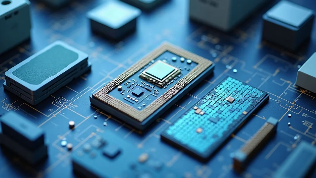
What is Advanced Packaging for Semiconductors?
Answer:
Simply put, advanced packaging for semiconductors is the use of innovative, multi-layer assembly formats like panel level, wafer level, and 3D integration to optimize the performance, density, and size of semiconductor devices. By leveraging finer control over die placement, redistribution layer formation, and multi-chip stacking, manufacturers enable higher device performance in smaller footprints. However, the increased complexity of these methods drives the need for even more sophisticated semiconductor inspection solutions throughout the process.
Inspection Needs Created by Miniaturization and Complexity
The miniaturization trend in semiconductor packaging pushes both size and precision limits, magnifying the consequences of undetected defects. As die level parts decrease to sub-millimeter scale and wafer level interconnects pack even closer, routine visual inspections become nearly impossible. Problems like foreign material inclusions, patterning errors, and flux deposit inconsistencies demand technological solutions well beyond manual or legacy equipment. Thus, advanced inspection systems—combining optical, X-ray, and even AI analysis—have become the backbone of modern quality control in packaging lines.
What is Semiconductor Inspection?
Answer:
Semiconductor inspection encompasses automated and manual processes designed to detect, classify, and trace defects throughout the chip manufacturing and packaging lifecycle. Its purpose is to verify that each die, wafer, or packaged device meets tight technical and reliability standards. Advanced inspection systems conduct non-destructive tests using a variety of optical, electrical, and metrology tools. For advanced packaging, inspection takes place at multiple steps—from initial die placement to level integration—helping manufacturers reduce false call rates, catch process drift, and ensure robust electrical connections.
Core Capabilities of Advanced Semiconductor Packaging Inspection Systems
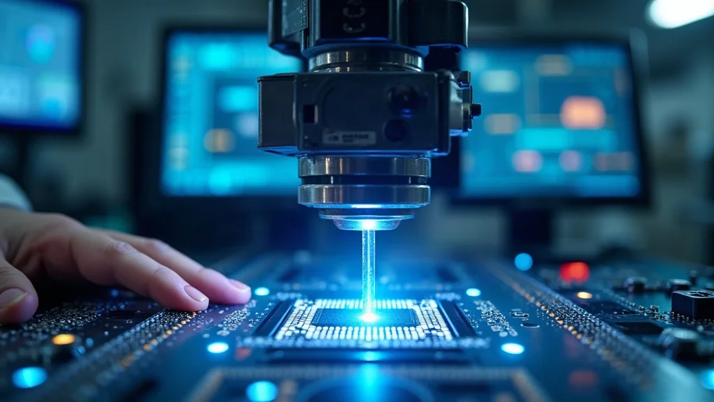
The heart of a modern inspection system is its ability to not only spot visible and sub-visible defects but also supply actionable data for process feedback. Capabilities include high-resolution imaging, real-time defect classification, advanced pattern recognition, and seamless data logging for traceability and regulatory compliance. Today’s inspection systems integrate IoT-enabled sensors and AI to enhance predictive maintenance and process optimization. For plant managers and operations teams, this means faster root-cause analysis, lower scrap rates, and higher value per processed wafer or panel.
Why Inspection Systems Are Critical to Advanced Packaging Success
Key Defects Detected by Semiconductor Inspection Systems
Shorts and opens
Delamination
Alignment errors
Foreign material inclusions
Patterning defects
Role of Inspection in Yield Improvement and Cost Control
Superior inspection systems aren’t solely about defect detection—they enable yield improvement and provide cost leverage. By identifying faults early (such as delamination or flux deposit issues), inspection prevents defective units from contaminating final output, reducing rework and scrappage. For high-throughput die level and panel level lines, a single missed alignment error may impact thousands of units. Comprehensive measurement data supports process engineers in making evidence-based changes to the manufacturing process, ultimately reducing operational expenses and boosting first-pass yield rates.
"By pinpointing problematic steps with precision inspection, we’ve seen direct yield improvements of several percentage points, with ripple effects through our supply chain and customer satisfaction scores." — Senior Process Engineer, Leading Foundry
Industry-Leading Solutions: Advanced Semiconductor Inspection System Comparison
System |
Detection Accuracy |
Throughput |
Use Cases |
Integration Ease |
Inspection Technology Type |
|---|---|---|---|---|---|
System A |
Sub-micron |
High |
Panel level, wafer level |
Plug-and-play |
Optical + AI |
System B |
~1 micron |
Moderate |
Die level packaging, flip chip |
Custom integration |
X-ray, visual |
System C |
Sub-micron |
Very High |
High-volume wafer level |
Modular |
Hybrid (Optical/X-ray) |
Overview of Competing Approaches in Inspection Systems
The market offers a variety of semiconductor inspection systems, each catering to different packaging formats and production needs. Some prioritize ultra-high-resolution defect detection for die level and panel level processing, while others focus on speed and minimal operator intervention. New systems increasingly leverage AI for real-time pattern recognition and process drift alerts. When evaluating solutions, consider factors like integration with facility MES, data traceability, and support for non-destructive testing, as these can markedly affect both yields and total cost of ownership.

Which Companies Are Known for Their Advanced Semiconductor Packaging?
Answer:
Major industry players advancing panel level and wafer level packaging include:
Market Leaders in Panel Level and Wafer Level Packaging
TSMC
ASE Group
Amkor Technology
Intel
Samsung
These leaders set benchmarks in integrating inspection systems into high-complexity packaging lines, often driving the adoption of next-generation process control techniques and raising the bar for semiconductor inspection globally.
Does TSMC Do Advanced Packaging?
Answer:
Yes, TSMC (Taiwan Semiconductor Manufacturing Company) is renowned for its advanced packaging services. It offers leading-edge panel level and wafer level solutions that include technologies like CoWoS (Chip-on-Wafer-on-Substrate) and InFO (Integrated Fan-Out). TSMC’s efforts have solidified its status as a global technology leader in the semiconductor industry.
TSMC's Role in Driving Inspection Standards and Technology
TSMC’s internal standards for inspection are among the strictest in the world, especially regarding panel level and wafer level packaging. By collaborating with toolmakers, TSMC helps develop new semiconductor inspection systems that are quickly adopted industry-wide. This continuous innovation ensures that even as advanced packaging complexity increases, defect rates are kept exceptionally low, with lessons filtered out to the rest of the ecosystem.

What to Consider Before Investing in Advanced Semiconductor Packaging Inspection Solutions
Key Questions for Manufacturers and Operations Leaders
Is your existing equipment compatible with next-generation inspection systems?
What are your data handling and traceability requirements?
Will facility modifications be necessary to support new systems?
How do you evaluate the cost of ownership against expected value?
What change management and operator training needs do you face?
Potential Mistakes, Limitations, and Implementation Pitfalls
Common pitfalls include underestimating facility space requirements, neglecting to address data integration with MES/ERP, and insufficient training for operators, all of which can undermine the benefits of an advanced semiconductor packaging inspection system. Decision-makers should be wary of false call rates from poorly tuned inspection algorithms, as well as the risk of selecting systems that cannot scale with future process changes or packaging technique innovations. Avoid shortcuts: a short-term cost saving can result in long-term quality or throughput losses.
Lists of Practical Specifications and Buying Guidelines
-
Checklist: Evaluating a Semiconductor Inspection System for Your Facility
Compatible with your existing process and packaging formats?
Detection accuracy meets your product standards?
Integration support with factory MES and traceability systems?
Throughput matches projected production volumes?
Vendor support for installation, calibration, and ongoing training?
-
Questions to Ask Vendors About Advanced Packaging Inspection
How is the system calibrated for different wafer and panel sizes?
Can it detect key defect types (delamination, shorts, opens, patterning errors)?
What ongoing maintenance, software updates, and training does the company offer?
How does the system support AI/automation features and future expansion?
Key Takeaways: Advanced Semiconductor Packaging Inspection for Buyers
Advanced semiconductor packaging inspection drives both quality and business value
Successful implementation requires technical due diligence and real-world case assessment
Industry leaders set benchmarks for process and technology
Frequently Asked Questions About Advanced Semiconductor Packaging Inspection
Why are inspection systems essential in semiconductor assembly?
Inspection systems are crucial because they ensure every packaged device meets strict quality and reliability requirements, catching defects early in the manufacturing process to reduce scrap, rework, and field failures. By enabling real-time detection, they support overall yield improvement and facilitate data-driven process optimization for advanced, complex packaging lines.Can legacy inspection tools keep up with advanced packaging?
Legacy tools often fall short in detecting minute or sub-surface defects seen in modern wafer level, panel level, and 3D-packaged devices. As die sizes shrink and complexity grows, only next-generation semiconductor inspection systems offer the needed resolution, integration, and data capabilities to support process control and minimize false call rates.What is the ROI timeframe for new inspection systems?
While ROI depends on your facility’s output and baseline defect rates, many users observe measurable improvements in yield and defect reduction within the first several months post-installation. The most significant gains come from reducing scraps, rework, and liability costs by catching defects as close to their source as possible.
Industry Voices: What Manufacturers Are Saying About Advanced Packaging and Inspection
"After deploying an advanced inspection system in our level packaging line, we saw a marked decrease in false calls and a faster feedback loop for process adjustments. The upfront effort in vendor selection and operator training paid for itself through improved quality control and customer satisfaction." — Operations Manager, Major Semiconductor Manufacturer
See Advanced Semiconductor Packaging Inspection in Action
Plant Tour of a Modern Semiconductor Packaging Line Using Advanced Inspection
Interview With an Application Engineer on Inspection Challenges and Success Stories
Looking Forward: The Evolution of Advanced Semiconductor Packaging Inspection
Anticipated Developments in AI and Automation for Inspection Systems
The future of semiconductor inspection points toward smarter, more autonomous systems powered by AI and machine learning. Real-time analytics, predictive maintenance, and adaptive algorithms promise ever-higher throughput and defect detection rates for both wafer level and panel level lines. Enhanced robotic automation could allow for seamless line reconfiguration and new packaging format support, ensuring that inspection technologies keep pace with growing device complexity and shrinking form factors.

How Buyer Expectations and Market Demands Are Shaping Future Solutions
Buyer expectations are shifting toward “plug-and-play” systems with rapid ROI, easy data integration, and robust traceability. Market competition is pushing suppliers to offer not only traditional inspection system capabilities but also cloud-enabled analytics, automatic defect classification, and scalable integration for future process nodes. Manufacturers evaluating new systems should consider not only technical features but also the degree of vendor support, system flexibility, and upgradeability to secure long-term value and adaptability in a fast-evolving market.
Ready to Navigate the Future of Advanced Semiconductor Packaging Inspection?
Have industry insights or news tips? Reach out and join our network of global trade professionals today! Schedule your interview with Global Trade News.
As the semiconductor landscape continues to evolve, staying informed about global trade developments and regulatory shifts is essential for forward-thinking manufacturers and supply chain leaders. For a broader perspective on how international markets, policy changes, and technology trends are influencing the future of advanced packaging and inspection, explore the latest insights and expert analysis at Global Trade News. Whether you’re seeking to anticipate market disruptions or identify new growth opportunities, leveraging up-to-date intelligence can help you make smarter, more resilient business decisions in this dynamic industry.





Write A Comment