









Imagine a modern semiconductor fab, humming with advanced machinery, where every silicon wafer that passes through the line has the potential to make or break a product schedule. Every step, from initial inspection to final yield review, plays a critical role in determining whether millions of chips emerge flawless—or whether costly defects slip through. In today’s fiercely competitive environment, mastering the craft of inspection and yield management is the key to operational excellence. This guide reveals how manufacturers can systematically reduce defects and optimize outcomes, no matter the company’s size or technological maturity.
Inspection and Yield: A Guide to Reducing Defects in Semiconductor Manufacturing
The inspection and yield process is not just a technical requirement but a business imperative for semiconductor manufacturers. By prioritizing effective yield management, ops leaders and engineers can address core issues leading to yield loss, optimize data collection strategies, and use predictive maintenance to keep operations running at peak performance. A robust inspection and yield management solution focuses on uncovering the sources of defects—whether due to physical contamination, electrical anomalies, or process variations—before they impact your bottom line. Leveraging advanced tools and analytics, manufacturers gain not just visibility but actionable insight into the production process. Ultimately, the objective is to improve wafer yield, raise the pass rate, and drive competitive advantage in a global supply chain increasingly dependent on defect-free production.
What You'll Learn
The role of inspection and yield in semiconductor manufacturing
Common sources of manufacturing defects and how they impact yield
Effective strategies for data collection and analysis
How predictive maintenance can improve yield and reduce downtime
Case studies of successful yield management in action
Frequently asked questions about yield, inspection, and defect reduction
Understanding Inspection and Yield in Semiconductor Manufacturing

Defining Inspection and Yield
At its core, inspection in semiconductor manufacturing involves systematically examining wafers for defects at various stages of the fabrication process. These checks might be visual, automated, or analytical, but the goal is always to detect issues—like scratches, particles, or open circuits—early and often. Meanwhile, yield measures the ratio of functional units—chips, dies, or wafers—that emerge from the production line compared to the total produced. A higher yield means fewer defects and better profitability. The term “yield management” describes the entire process of improving this ratio, from root-cause analysis to process optimization and predictive maintenance. Manufacturers rely on yield analysis tools and integrated inspection data to pinpoint where the process steps introduce defects and to take targeted action for yield improvement.
Why Yield Management Is Critical to Semiconductor Success
In the world of high-volume semiconductor production, even a 1% increase in yield can spell millions in revenue and substantial competitive gain. Yield management ensures that problems are identified swiftly and remedied before they escalate, protecting against yield loss and unplanned downtime. Inspection data collected throughout the manufacturing process feeds analytics and decision-making, highlighting where process improvements or equipment upgrades are most urgently needed. Manufacturers that excel at yield management typically outperform their peers in quality, cost, and delivery, cementing stronger positions in global supply chains.
"Yield management is the backbone of high-volume semiconductor production. Every percentage point in yield improvement directly impacts profitability and competitive advantage."
Common Defect Types in Semiconductor Manufacturing and Their Causes
Introducing Inspection and Yield Challenges
Understanding the root causes of yield loss requires a comprehensive approach to data collection and analytics. In a modern fab, wafers undergo hundreds of intricate process steps, each one introducing new risks for physical, electrical, or process-related defects. Manufacturers often face challenges in distinguishing between random defects—linked to chance events—and systematic defects caused by equipment malfunctions or process drift. Continuous improvement depends on separating the two and deploying advanced inspection systems and analytics to catch and correct problems before they mount.
For manufacturers seeking to deepen their understanding of how global trade dynamics and regulatory shifts can impact semiconductor supply chains and defect management, exploring the latest insights on trade regulations and market trends can provide valuable context for operational decision-making.
Physical Defects: Scratches, Particulates, and Contamination
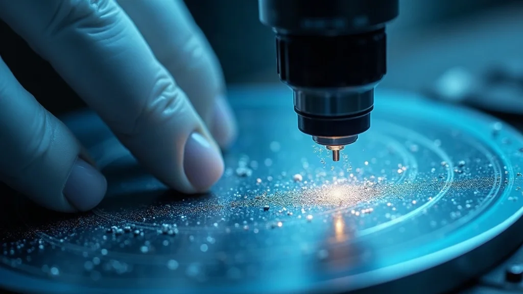
Physical defects arise from contamination, mechanical damage, or uneven material deposition. Scratches can originate from improper wafer handling, while particulates may be introduced by airborne dust, human contact, or suboptimal cleanroom conditions. Contamination impacts not only yield but also long-term product reliability, requiring process step controls and high-grade inspection methods. High-frequency inspection at critical process steps reduces the risk of defects progressing undetected downstream. Inline vision systems, advanced cleaning protocols, and rigorous operator training are all essential elements for minimizing physical defects in semiconductor manufacturing.
Electrical Defects: Opens, Shorts, and Leakage
Electrical defects, such as opens, shorts, or leakage currents, often occur due to lithography misalignments, etching errors, or deposition failures. These can cause integrated circuit elements to malfunction or render entire wafers unfit for further processing. Regular wafer test routines allow for deep analysis of circuit integrity. Results from test data inform yield management and guide process improvements, making electrical inspections at both inline and end-of-line stages essential for high pass rates. Companies also leverage advanced tools and neural network algorithms to detect subtle electrical issues hidden in vast volumes of process and test data.
Process Variations and Their Impact on Inspection and Yield
Photolithography errors: misalignment, blur, resist thickness variations
Etching problems: under/over-etch, profile deviation
Deposition inconsistencies: film thickness variation, contamination
Doping and diffusion failures: non-uniform doping, incorrect diffusion profiles
Even when defects are not immediately visible or electrically catastrophic, slight deviations in process steps can compound through the manufacturing process, gradually eroding yield. Continuous data collection and statistical process control help fabs detect these subtle trends. Machine learning methods—like time series forecasting using neural networks—now play an increasing role in predicting and intercepting emerging defect trends.
Inspection and Yield: Steps to Identify and Reduce Defects

Why Data Collection Is Fundamental for Yield Management
Data is the foundation of modern yield management. From the moment a wafer undergoes its first process step, data should be captured—covering equipment conditions, materials used, environmental parameters, and outcomes of key inspections. Comprehensive information collected across all stages enables manufacturers to identify correlations between process variables and defect rates. Maintaining high data integrity and accessibility is essential, as yield optimization relies on both breadth (monitoring every process step) and depth (analyzing nuanced test data). The semiconductor industry increasingly views robust data collection as a competitive differentiator as well as an operational safeguard.
Inline and End-of-Line Inspection Systems

Automated inline inspection systems provide real-time visibility at each major process step, flagging defects as soon as they occur. High-speed optical scanners, X-ray imaging, and electron microscopes capture defects at resolutions beyond human capability, drastically improving catch rates for both physical and electrical issues. At the end of the production line, end-of-line inspection and wafer test procedures verify that the completed products meet quality standards. Test data from these stages forms the basis for both immediate corrective action and long-term process improvement. As the complexity of integrated circuits grows, so too does the importance of layering advanced inspection methods with smart analytics for comprehensive defect detection.
Implementing Predictive Maintenance to Prevent Defects
Predictive maintenance uses real-time machine data and advanced analytics to forecast when equipment may drift out of its operational tolerances—well before failures cause product defects or downtime. Unlike scheduled maintenance, which is calendar-based, predictive programs use actual site performance and sensor readings to trigger just-in-time service or part replacement. By addressing process anomalies promptly, predictive maintenance reduces the potential for yield loss due to equipment-induced defects. The result? Fewer interruptions, greater pass rates, and a production process that consistently meets tight quality control targets. Integration of machine learning and even deep learning models further enhances the accuracy of defect prediction and maintenance decision-making.
Using Advanced Analytics for Yield Analysis
Yield analysis incorporates data from inspections, test equipment, and process monitoring to create a detailed picture of fab performance. Using advanced tools—including data mining, neural networks, and AI—engineers can find hidden defect patterns, connect them to process variables, and strategize targeted improvements at the process step most likely to influence lower yield. High-impact yield improvement hinges on putting analytics front and center. Data visualization dashboards, automated alerts, and digital twin simulations help teams make sense of complex multivariate data faster, ensuring that both material and capital resources are directed where they have the greatest impact.
Techniques for Reducing Defects and Improving Inspection and Yield |
||
Technique |
Main Benefit |
Application |
|---|---|---|
Inline Inspection |
Early detection and correction of defects |
Wafer handling, photolithography, deposition |
Data Collection & Integration |
Deeper defect pattern recognition |
All process steps, equipment, environmental factors |
Predictive Maintenance |
Minimize unplanned downtime, proactive repairs |
Critical production equipment, sensors, cleaning stations |
Advanced Analytics |
Pinpoint process step yield loss |
Automated dashboards, AI-driven analysis |
The Data-Driven Approach: Using Data Collection to Optimize Inspection and Yield
Effective Data Collection Methods in Modern Fabs
Modern semiconductor fabs derive much of their competitive advantage from sophisticated data collection. Every wafer undergoes hundreds of process steps, each one logged for input variables, inspection results, and machine states. Automated sensor networks streamline the process, ensuring that data is reliable, up-to-date, and immediately available for analysis. Best-in-class fabs use sensors and industrial IoT gateways to capture everything from environmental cleanliness to tool vibration and energy use. By consolidating this information in unified databases, they enable cross-functional yield management teams to collaborate effectively and respond rapidly to emerging defect trends.
Analysis Tools for Yield Management

Effective yield management solutions depend on cutting-edge analysis tools to make sense of large and complex data sets. Platforms with AI capabilities—such as neural networks and machine learning analytics—are increasingly standard, as they provide actionable insights from time series test data and process logs. Key functions include anomaly detection, root-cause analysis, predictive defect modeling, and yield forecasting. These advanced tools integrate with fab systems to deliver real-time feedback, so process engineers and operators can adjust parameters quickly. For many operations leaders, the right yield management solution translates directly into fewer yield losses and higher production quality.
Integrating Data with Predictive Maintenance Systems
Merging robust data collection with predictive maintenance amplifies yield gains and reduces risk. Real-time process and equipment data feed into predictive models, which in turn indicate exactly when intervention is required. This closed-loop approach produces significant savings in both downtime and scrap, allowing fabs to move toward a zero-defect goal. Successful integration also depends on aligning maintenance and production teams, investing in cross-training, and developing standard procedures for interpreting and acting on system alerts. The more seamless the integration, the more effective your yield management program becomes.
"Combining real-time data collection with predictive maintenance allows for unprecedented yield gains and operational efficiency." — Industry Expert
Predictive Maintenance: Minimizing Defects for Higher Inspection and Yield
Principles of Predictive Maintenance in Semiconductor Manufacturing
The core principle of predictive maintenance is simple: anticipate failure before it causes site performance issues or yield loss. Using continuous sensor streams and historical time series data, predictive models—often built with neural networks or other machine learning approaches—detect small signals that precede major tool failures. Applying predictive maintenance in semiconductor manufacturing improves both equipment uptime and product pass rates. Instead of reacting to breakdowns, your team can schedule maintenance based on need, maintaining optimal performance and keeping yields high through every fabrication process step.
Real-World Predictive Maintenance Applications

In one real-world case, a major U. S. -based fab implemented AI-driven predictive maintenance across its photolithography and etch tool fleets. By integrating real-time vibration, temperature, and output data, the fab reduced unscheduled downtime and caught tool drifts before wafer-level defects escalated. Such applications demonstrate that predictive maintenance is not just theoretical, but a proven method for improving both inspection and yield. Savings are seen in minimized scrap, consistent wafer yield improvement, and lower costs for urgent repair and replacement parts.
Benefits of Predictive Maintenance on Yield Management
Manufacturers that embrace predictive maintenance realize multiple benefits: higher pass rates, less yield loss, more efficient labor allocation, and stronger competitive positioning in tight global markets. Moreover, predictive programs can be scaled across different fabs, equipment types, and even worldwide sites—helping U. S. and international companies meet demand for ever-smaller, more reliable integrated circuits. Predictive analytics tools also feed process step-by-step insights into broader yield management strategies, increasing the whole operation’s agility and responsiveness as market and technology demands change.
Lessons Learned: Common Pitfalls to Avoid
Despite its clear benefits, predictive maintenance programs sometimes stumble due to lack of buy-in, inadequate data collection, or misaligned goals. Successful yield management relies on executive support, well-defined objectives, employee engagement, and continual review of maintenance accuracy versus actual yield outcomes. It’s vital to avoid underestimating both the technical and cultural shifts required for broad adoption—ranging from reworking reporting lines to investing in robust training and change management frameworks.
Yield Management in Action: Case Studies of Defect Reduction
Case Study: Major Fab Implements Inspection and Yield Solution

A prominent semiconductor manufacturer, headquartered in the United States, set out to overhaul its yield management process after experiencing a lower yield trend across its flagship product line. By deploying a new inspection and yield solution—focused on real-time data collection, AI-powered analytics, and integrated predictive maintenance—the fab achieved tangible improvements within six months. The transformation began with baseline data mapping, followed by systematic upgrades to inline inspection systems and equipment sensors. Neural network algorithms identified recurring yield loss sources, especially in wafer test stages previously thought to be robust. Management invested in hands-on cross-functional training to ensure each process step team could interpret analytic results and act on predictive alerts.
Improved Yield Analysis and Measurable Results
Within months, the fab’s updated yield management solution delivered a measurable increase in wafer yield and a consistent upward pass rate trend. The company not only reduced scrap and rework expenses, but also accelerated new product ramp and improved customer satisfaction scores. Frequent use of advanced analysis tools allowed rapid deployment of corrective measures whenever defect or downtime risks arose, illustrating the value of real-world continuous improvement.
"Our investment in robust yield management tools paid off rapidly, enabling faster ramp and improved customer satisfaction." — Fab Manager
Best Practices and Strategies for Inspection and Yield Improvement
Leadership and Team Engagement in Inspection and Yield Initiatives

No matter how advanced your analytics or inspection systems, sustainable yield gains start with leadership commitment and cross-functional teamwork. Top-performing fabs task yield 'champions' at each process step, foster open communication, and empower all staff to flag and troubleshoot sources of yield and defect. Regular knowledge-sharing and continuous education ensure that both experienced engineers and newer hires are adept at using data, analytics, and predictive maintenance platforms. Setting clear objectives and tracking progress are vital to maintaining momentum in inspection and yield improvement programs.
Process Optimization: From Data Collection to Yield Management
Process optimization does not happen overnight—it’s an ongoing cycle: collect, analyze, act, and iterate. Advanced tools like machine learning and neural networks help uncover hidden yield loss patterns in high-volume data streams. Industry leaders stress the importance of capturing information at every process step, validating key insights, and involving teams across disciplines. Whether you are a large U. S. fab or a smaller global player, deploying stepwise upgrades to both equipment and analytics platforms makes yield gains achievable and sustainable. Focus on continuous refinement, and remain open to lessons from both internal audits and industry benchmarks.
-
Top 5 Mistakes to Avoid in Yield Management:
Failing to invest in comprehensive data collection across all process steps
Ignoring training and change management for frontline operators
Allowing siloed teams to manage inspection and yield in isolation
Delaying action on predictive maintenance alerts
Over-relying on outdated analysis tools when advanced options are available
-
Essential Steps Before Deploying a Yield Improvement Program:
Map and assess existing inspection systems and data flow
Benchmark current pass rates and identify yield loss hotspots
Review workforce skills and invest in targeted training initiatives
Collaborate with vendors to ensure technology scalability and integration
Establish a regular review cadence for lessons learned and progress tracking
Technology Choices: What to Look for in Inspection and Yield Solutions
Evaluating Different Yield Management Technologies

Selecting the right inspection and yield management solution is a major factor in reducing defects and maintaining production quality. Technologies should be evaluated based on their ability to deliver rapid, high-resolution data collection, integrate with existing fab infrastructure, and adapt to new process requirements as product demands evolve. Look for solutions that offer robust analytics—preferably those employing AI, machine learning, or time series neural network capabilities—and ensure they can scale across multiple process steps and fab sites. Partnering with vendors who provide deep industry expertise and post-deployment support is equally important.
Cost, Scalability, and Integration Factors
When choosing between yield management solutions, manufacturers must balance up-front investment with long-term ROI. Consider the total cost of ownership, including maintenance, licensing, and training. Scalable platforms allow for incremental upgrades as production volumes and complexity increase, ensuring your solution grows with your business. Integration with existing MES (Manufacturing Execution System) and automated inspection tools streamlines workflow and minimizes disruptions during rollout. Effective partnership with IT teams, equipment suppliers, and process engineers is vital for successful implementation.
Addressing Implementation Challenges in Data Collection and Predictive Maintenance
The most common implementation hurdles revolve around data integration, change management, and aligning predictive maintenance schedules with fab priorities. A phased rollout, robust pilot testing, and transparent leadership communication make the transition smoother. Investing in employee training and change management resources will accelerate adoption and improve results. Remember, even the best technology falters without skilled teams and well-defined business processes. Prioritize internal stakeholder buy-in and sustained engagement to ensure program success.
Comparison of Leading Yield Management Approaches and Tools |
||
Approach/Tool |
Key Strength |
Considerations |
|---|---|---|
Automated Inspection Systems |
Consistent, high-speed defect detection |
Requires significant up-front investment |
Integrated Data Analytics Platforms |
Real-time defect and yield insights |
Complex integration with legacy systems may be needed |
Predictive Maintenance Tools |
Early warning for process anomalies |
Dependent on quality and granularity of collected data |
AI/Deep Learning Solutions |
Advanced pattern detection in big data |
Requires skilled staff for model training and validation |
Training, Change Management, and Continuous Yield Improvement
Building Internal Expertise on Inspection and Yield

Building internal expertise is the foundation of lasting change. Ongoing training ensures that staff at every level—from operators to plant managers—can effectively interact with inspection platforms, interpret analytics, and act on predictive maintenance recommendations. Experienced engineers should mentor newer hires, passing along both technical know-how and problem-solving skills. A learning-focused environment helps organizations retain valuable talent and adapt to evolving yield management practices.
Establishing a Framework for Continuous Yield Management
Continuous improvement is a mindset as much as a methodology. Leading manufacturers set clear KPIs for inspection and yield, review progress in routine meetings, and foster open channels for feedback between teams. Success is tracked not only in rising pass rates, but also in reduced scrap, shorter ramp times, and less downtime. In addition to regular reviews, organizations often create rotating roles or 'yield task forces' to keep improvement initiatives fresh and relevant as the product mix changes and technologies advance.
Case Example: Change Management Success in Predictive Maintenance
One U. S. semiconductor fab faced resistance when rolling out predictive maintenance for critical cleaning tools. By including operators in the design of monitoring dashboards and holding joint workshops with IT, operations, and engineers, the fab built widespread engagement—and saw both defect rates and unplanned tool downtime fall significantly. This success shows that change management is as crucial as the tools themselves and underscores the value of employee-led approaches to technology adoption.
The Future of Inspection and Yield: Semiconductor Trends and Innovations
Emerging Technologies in Inspection and Yield

The next wave of inspection and yield management is being shaped by innovations in artificial intelligence, machine learning, and the industrial internet of things. AI-powered platforms deliver instant analysis, anomaly detection, and even prescriptive actions—reducing cycle times and maximizing uptime. Global manufacturers are testing augmented reality for onsite support, deploying more adaptive sensor networks, and experimenting with quantum-inspired algorithms for even deeper yield insights. Staying ahead means being willing to continuously evaluate and adopt emerging technologies as they mature.
AI, Machine Learning, and Beyond
As neural networks and deep learning architectures become more accessible, their applications in defect pattern recognition, outlier detection, and predictive analytics are rapidly expanding. These advanced tools can sift through massive data sets and reveal subtle yield loss correlations that traditional analytics might miss. Machine learning integration is moving beyond isolated projects and becoming part of core yield management solutions—pushing the boundary for what’s possible in defect reduction and fab optimization. For many global fabs, embracing these technologies is critical to long-term competitiveness.
Global Collaboration for Better Yield Management
Inspection and yield is increasingly a global pursuit. Partnerships between U. S. fabs, Asian OEMs, and European analytics providers are fueling advancements in both tools and best practices. Data and know-how flow freely in these partnerships, accelerating innovation and establishing higher industry benchmarks. This collaborative momentum suggests a future where digital transformation is not just an individual fab asset, but an industry-defining trend.
"Ongoing digital transformation is set to redefine inspection and yield control processes for the industry as a whole."
People Also Ask
What does yield mean in the semiconductor industry?
Understanding 'Yield' in the Semiconductor Context
In the semiconductor industry, yield is the percentage of functional chips or devices produced from the total output in a fabrication process. This measurement reflects the effectiveness of inspection and yield management strategies during integrated circuit production. High yield indicates fewer defects and greater operational efficiency, which translates directly to higher profitability for manufacturers and more reliable products for customers.
What is the yield test?
Defining The Yield Test and Its Role in Inspection and Yield
The yield test is a comprehensive set of evaluations performed on wafers after major processing steps to determine the number of usable chips produced versus the total tested. This process involves functional, parametric, and sometimes reliability assessments, with inspection results shaping the direction of future process improvements. Yield testing is a critical aspect of both pass rate tracking and identifying areas where defect rates may be increasing, enabling proactive adjustments to maintain high production quality.
What is yield analysis?
Yield Analysis for Monitoring Inspection and Production Performance
Yield analysis is the methodical examination of process and test data to measure, monitor, and enhance manufacturing effectiveness. By reviewing each process step, manufacturers can pinpoint sources of lower yield and implement corrective actions. Modern fabs use data analytics, sometimes powered by machine learning or deep learning, to continuously improve inspection precision and maximize the functional output of every production run.
What is the formula for calculating wafer yield?
Calculating Wafer Yield: Formula and Practical Application in Yield Management
The basic formula for wafer yield is: Yield (%) = (Number of Functional Dies / Total Dies on Wafer) x 100. This calculation gives a clear percentage indicating how successfully the manufacturing process produced usable chips. By analyzing yield data after each major processing step, teams can identify when and where defects occur and refine both inspection techniques and predictive maintenance routines for optimal results.
Frequently Asked Questions About Inspection and Yield
How does predictive maintenance reduce semiconductor defects?
Predictive maintenance works by monitoring the real-time performance of manufacturing equipment and using analytics to forecast potential failures. By proactively addressing issues before they cause defects, manufacturers maintain high process integrity and minimize both unplanned downtime and yield loss. This preventative approach is critical in a complex production process with hundreds of variables affecting wafer quality.
What data should be collected for effective yield management?
Effective yield management relies on capturing information collected at every process step, including environmental conditions, equipment settings, inspection results, and test data from each wafer batch. Detailed and comprehensive data enables deeper analysis, accurate identification of root causes for defects, and timely responses that keep yield levels high.
Are there industry standards for measurement in inspection and yield?
Yes, multiple industry standards—such as ISO 9001 and SEMI standards—define protocols for inspection, test data integrity, pass rate calculation, and continuous improvement programs. Compliance ensures reliable yield comparisons and supports efforts to benchmark site performance, optimize defect control, and implement best practices across the supply chain.
How can small and medium manufacturers benefit from advanced yield management tools?
While advanced yield management solutions are often associated with large, global fabs, smaller and medium-sized manufacturers can also benefit. Scalable data collection platforms, AI-powered analytics, and predictive maintenance programs help these operations identify and address defects efficiently, making them more competitive in both domestic and international markets. Strategic investment in these technologies supports steady growth and higher production reliability.
Key Takeaways for Effective Inspection and Yield Improvement
Inspection and yield are central to reducing defects and maximizing output.
Data collection and analytics power effective yield management.
Predictive maintenance is an essential tool for proactive defect reduction.
Case studies demonstrate measurable benefits and lessons for manufacturers.
A thoughtful approach to technology, training, and management is vital for success.
To stay ahead in the rapidly evolving world of semiconductor manufacturing, it’s essential to look beyond the fab floor and understand the broader forces shaping your industry. For a deeper dive into the latest developments in global trade, regulatory changes, and market opportunities that can influence your inspection and yield strategies, visit Global Trade News. Their expert coverage offers actionable intelligence and forward-looking perspectives, empowering you to make informed decisions that drive both operational excellence and strategic growth. Explore how external trends and policy shifts can unlock new avenues for yield improvement and competitive advantage in your organization.





Write A Comment